You may have seen this how to make a PCB but before making PCB you must have knowledge about how to make layout to make PCB.
There are various software by which you can make layouts like KiCad, OrCAD, eagle, spice etc. Here we will discuss about KiCad and use it to make layouts.
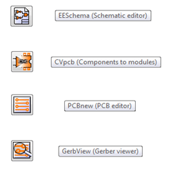
Here is a small introduction about KiCad which is very easy to use and somewhat easy to understand. In KiCad we have to follow a total of 4 steps to complete the PCB layout. These steps are shown in the image.
For brief details about KiCad, just search on Google!
1. EESchema (schematic editor) –
In this step, we have to draw the required circuit diagram.
two. CVpcb (components for modules)-
This step shows how to assign coverage areas to a specific component.
3. PCBnew (PCB publisher) –
Here you actually have to design the rails according to your wiring done in EESchema.
The track width can be adjusted according to our needs.
4. GerbView (Gerber Viewer) –
To send your card to a manufacturer you will need to generate a gerber file.
Fig. 1: Image showing icons of various KIcad components
See if the downloads start at the end.
Starting a new project
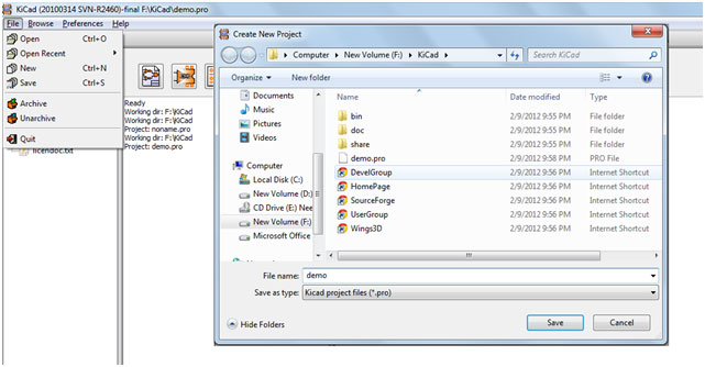
First we have to create our project file that we will work on. For example, demo. To do this, click on file>new>demo and press enter. Then the demo.pro file will be created. This “.pro” file extension indicates that it is a project file.
Fig. 2: Screenshot of creating a new project in KIcad
After creating the new project we have to click on the 1st EESchema icon which is shown in Fig.
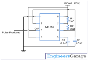
Now we will see all the steps in detail. But remember that you will get all the features of kiCad only by practicing it more and more. Here we will take an example to make PCB. Circuit is the generation of sound in the audio track of the Engineergarage website itself. ( )
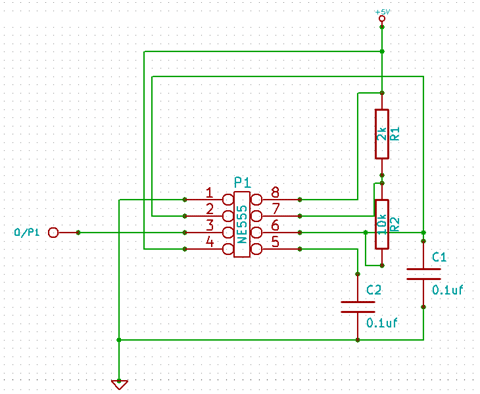
Circuit Diagram-

Fig. 3: Circuit diagram of a 555 IC based design
Step 1: EES scheme
STEP 1: EES scheme
Now click on the EESchema i.e. 1st icon . The new window will appear to draw the schematic of any circuit. We have an example circuit diagram taken from the web as above.
It will show some error like demo.sch (in the above case) not found. Ignore it and click OK. Here the “.sch” extension indicates your schematic file. The new window will look similar to below. Now zoom in and we will get the grids where we should draw our scheme.
Save the schema. Configure the page and enter the title of the scheme. You can give whatever you want.
To draw the schematic we have to place the components on the provided sheet. To do this, click on location> component. The component window will appear. In it you can select components from the list. Even to install a resistor, you can simply write “R” and click on the search keyword. Double click on that component and it will be placed on the worksheet. You can browse the category view of the components. If there are some devices/components missing, try adding library files to your drive where KiCad is installed: KiCadsharelibrary. Therefore, you must copy these libraries to the library folder. You can download libraries by searching for them on Google, like the NE555 KiCad library. According to your circuit diagram, make the schematic.
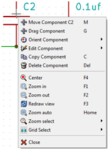
Place the cursor on the component and right-click on it. From this list you can delete, edit, move and rotate the component according to your need. Similarly, to select LED, just search for LED or you can put it in the list. After completing your schematic, save it.

Fig. 4: Screenshot of saving a schema by EESchema in KIcad
After arranging the components in the appropriate locations, it's time to connect them to the wire. Go to place > thread. Now you can connect more than 2 wired components. If there is a connection between 2 wires in the circuit diagram, in the schematic you will see the node (bubble) that shows that there is a connection. 1st step is almost complete here. If you want to add a node, click 'place a junction'.
As you did with the schema before assigning the spaces, you must give the components their own names. Since we took a small sample for demonstration, if the schema is much larger and contains many components, it will be difficult to provide proper names. Instead, there is a function to automatically annotate the schema. If you can see the icon indicating the annotation scheme, click it. If you are using a single sheet, don't change anything, just click on the note. Click the OK button. You will see that your entire scheme is written down!
To assign footprints we must create a netlist. Before the annotation icon there is an icon indicating the generation of the netlist. This netlist can be used in PCBnew, OrCAD, Spice etc. Don't change anything, click on netlist and save.
Now the scheme will look like below. Keep in mind that I drew it as in the circuit diagram to make it clear to you. You can draw it according to you, but make sure the connections are accurate.
(Note: I forgot to put the power supply connection for +5V, so you add it while drawing the schematic)

Fig. 5: Image of a schema designed by EESchema in KIcad
Save your work. Close the current worksheet. 1st stage is completed!
Step 2: CvPCB
STEP 2: CvPCB
In this step, we have to assign footprints to the respective components. It is very easy for components like capacitor and resistor because we can bend their leads but it is very difficult if we are to assign it to any DIP/QFP/SMD IC. Since there is a greater or lesser distance between the pins than the actual distance between the pins of the IC, our PCB may be useless. Therefore, care must be taken when assigning footprints.
Let's start with this step.
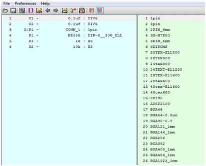
Open CvPCB. Click on OK button as it will show some error. You will see all the components you have in your schematics. Now, if you click on any component present in the left column, you will get a list of filtered footprints. Additionally, you will get unfiltered footprints in the right column. Click on any footprint and click view selected footprint.
You can see the distance between 2 pins. To make the calculation easier, right click > grid selection > 39.4 mils (1 mm). It is very useful to calculate the distance between 2 pins. You can get a 3D view of this footprint by clicking the 3D button. Close this window and get the proper space for your component. After that, double click on that area and it will be assigned to the respective component. We have our sample schematics so the assigned area looks like the following figure.

Figure 6: Screenshot of CvPCB in KIcad
Now click on create export file and click on save. Don't change your name or anything.

Fig. 7: Screenshot of creating the export file in CvPCB
You are done with 2 and step. Minimize or close the current window.
Step 3: New PCB
STEP 3: New PCB
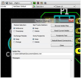
After opening PCBnew, you will see the reduced window. We created netlist file, here we need to read this netlist file to draw tracks. Click read netlist file and then click read current netlist. See only the Nelist Dialog window below, not behind it.
Fig. 8: Screenshot of PCBnew in KIcad
One point to keep in mind why I'm not showing all the icons is that you will become environmental with this software, which is the basic step to learning it.
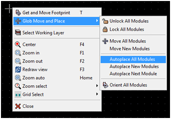
Ok, now your project will be in the top left corner of the spreadsheet. Zoom in. Now you must move on the sheet and place them separately as they come together after opening the window. To do this, see the following fig.
Fig. 9: Screenshot of automatic module placement in PCBnew in KIcad
Select the components and right-click on them. Then make the selection above. Autoplace All Modules will automatically place your modules in a systematic manner. Now comes the difficult step!
Focus on the connection between components. If you cannot see the connections, click on manual and automatic movement or module placement. After arranging the components in suitable locations, it's time to connect them to the rails. You can rotate the component if the connection is getting complicated. For the 1st time you can copy the tracks and the placement of the components like I did. While practicing, you can choose your vision. Click on add trails and roads. Click on any component pin and click on another pin that has a connection to that pin. If you made the connection, double click to fix that track.
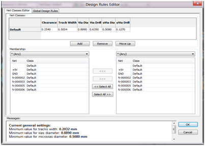
It is usually best to keep the track width to 1mm thick. As for students for practice, a track width of 1 mm thick is sufficient. If you are doing well, you can choose the appropriate trail width. To change the track width, click Design Rules and make changes to the track width. Enter the appropriate track width and click OK.
Fig. 10: Screenshot of the Design Rules Editor in KIcad
ONE THING TO TAKE CARE OF NOT DRAWING TRACKS WITH STRAIGHT LINES!!! THEY MUST BE DRAWN AT 45 degrees. THIS SOFTWARE WILL CUT THE LINE AT 45 DEGREE DURING MOTION. JUST MAKE SURE THE TRACKS ARE DRAWN AT 45 DEGREES AND DO NOT MATCH EACH OTHER. IF YOU ATTEMPT TO OVERLAY IT WILL NOT BE ACCEPTABLE BY THE SOFTWARE. IF THE DISTANCE IS TOO SHORT BETWEEN TWO CONNECTIONS, THIS TIME MAY DRAW WITH STRAIGHT LINE. THE REASON BEHIND YOU WILL KNOW LATER. AND YES, WE ARE MAKING SINGLE LAYER PCB. THIS SOFTWARE SUPPORTS MULTIPLE LAYER PCB, BUT WE TRIED SINGLE LAYER AT THIS TIME!
Fig. 11: Image showing right and wrong methods of creating a network
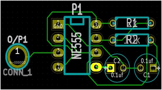
After following these instructions, you will know how to draw exact tracks. I drew it, so go through it if you're having trouble.

Fig. 12: Image of a PCB layout designed in KIcad
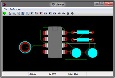
Here I assigned the footprint of a 1-pin connector with a much larger diameter. This is labeled CONN_1. When you go to assign the footprint make sure the diameter is about 1 to 1.5mm or if you have a 1 pin connector you can see the footprint of that. You can see the 3D view of this PCB by clicking the 3D View tab. Then enlarge the window and you will get a 3D view.

Fig. 13: Screenshot of the 3D viewer in KIcad
Now it's time to create the GERBER file. Click on plot and select Gerber and click on Plot. It will create a Gerber file that many organizations send to manufacturers. It will create the respective file and here we end with 2 and last or maybe last step for some users.
Step 4: GerbView
STEP 4:GerbView
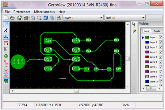
Why create a Gerber file? It is because there are many software that are used to make layouts. I said at the beginning that OrCAD, KiCad, Eagle etc software are useful for making layouts. The fact is that I use KiCad, but many manufacturers may use software other than KiCad. So Gerber file is a file that will help the manufacturer to know about your project and the manufacturer cannot make any changes in the Gerber file. There is now software that allows you to make changes to the Gerber file. Forget it, we are just apprentices. We don't have a big budget project, so it's not usable mainly for individuals. We can see the gerber file by clicking file > open and selecting any file we have already created.
Maker can see following views like top view and bottom view

Fig. 14: Gerbview screenshot in KIcad
Fig. 15: Gerbview screenshot in KIcad
After making a layout it's time to make PCB, but I think you knew how to do it. It has already been posted here by someone.
Transfers
Transfers-
1.Software –
The .exe file is for Windows and .tgz is for Linux
2. Libraries-
Or search for a specific library here
So friends, this is just the primary stage of doing the layout. In the background, there are many functions, such as assigning a custom footprint to any component if needed, not available, etc.
