In the previous tutorial of VHDL tutorial, we designed 8×3 encoder and 3×8 decoder circuits using VHDL.
(If you are not following this series of VHDL tutorials one by one, you will be asked to go through all the previous tutorials in this series before proceeding in this tutorial)
In this tutorial,
- We will write a VHDL program to build 1×8 demultiplexer and 8×1 multiplexer circuits
- Check the program output waveform (digital circuit) with the truth table of these multiplexer and demultiplexer circuits
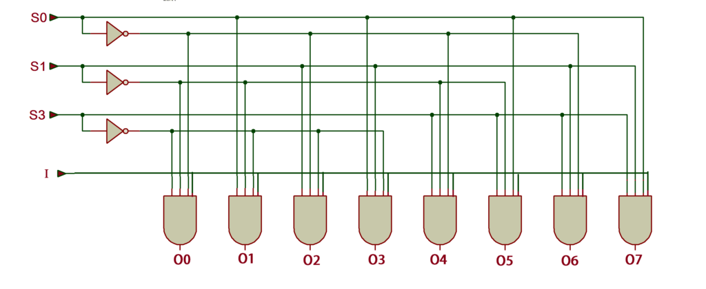
1×8 Demultiplexer Circuit
Truth table 
(Please follow the step-by-step procedure provided in the VHDL 3 tutorial to create a project, edit and compile the program, create a waveform file, simulate the program, and generate output waveforms.) Now let's write a VHDL program, compile it, simulate it and obtain the output in waveform. Finally, we will check if the output waveforms agree with the given truth table.
I used the behavioral modeling style to write a VHDL program to build the demultiplexer because it will be easier than the data flow or structural modeling style.
VHDL Program

(To learn more and get more details about the VHDL program(s), read the first two tutorials, VHDL Tutorial 1 and VHDL Tutorial 2 in this series.)
Then compile the above program – create a waveform file with all inputs and outputs listed – apply different input combinations – save the waveform file and finally simulate the project. You will get the following result.
Waveform simulation

As shown in the figure, it can be seen that when the selected lines (S2, S1, S0) are “001”, the input I=0 is available at the output O1=0, and when the selected lines are “101”, the input I =1 is available at output O5 = 1. You can check other combinations of selected lines with input and output.
Next, we will build an 8×1 multiplexer circuit.
8×1 multiplexer circuit

Truth table 
VHDL Program
 Simulation waveforms

As shown in the figure, it can be seen that for the selected lines (S2, S1, S0) “011” and “100”, the inputs d3=1 and d4=1 are available at the output o=1. You can check other combinations of selected rows from the truth table.
In the next tutorial, we will design clocked RS flip-flop and RS Latch.