

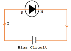
Biasing Techniques for PN Junction Diodes
- Direct bias
- Reverse polarization
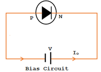
Forward-biased PN junction
When an external voltage applied to PN junctions is in a direction that disrupts the potential barrier and thus allows current to flow, it is called forward bias.
- To apply the concept of direct voltage, connect the positive terminal of the battery to the negative N-type terminal as shown in the figure.
- Once the battery is connected, the positive terminal of the battery repels the holes and the electrons are repelled from the negative terminal, causing both the electrons and the holes to be directed towards the junction where they reconnect.
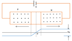
- Another way to explain current flow is in the forward direction. It can be said that due to the external voltage applied, the barrier potential is reduced which now allows more current to flow through the junction as shown in Fig.
W' < W
 When polarizing directly into the PN connection, the following points must be observed:
- The potential barrier decreases and is also canceled at a certain forward voltage (0.1 V to 0.3 V).
- The feature provides low direct resistance, R F, to the flow of electricity.
- Due to the formation of a conditional with low resistance, current flows in the circuit. The strength of the current depends on the applied direct voltage.
PN Junction ReverAnotherased
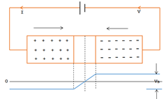
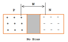
When an external voltage applied to the connection is divided into three so that the potential barrier is increased, it is called reverse voltage. When the battery connections are made to the semiconductor and conductor as shown in the figure, it is said to be in reverse bias condition.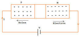
- In this case, holes are connected to the negative terminal of the battery and electrons are connected to the positive terminal, so both holes and electrons move away from the connection and away from each other as there is no connection of electrons and holes, no current flows and the join connection offers high resistance.
- Another way to analyze the method is that, in this case, the applied voltage increases the potential of the barrier, blocking the movement of most carriers, as shown in the figure.
- It should also be noted that the width of the barrier layer increases under reverse voltage conditions because most of the charge carriers are moved away from the connection. This also increases the potential barrier, as shown in FFig. showing.
 When using a reverse voltage for PN junction, the following points must be taken into consideration:
- The potential barrier is increased.
- The connection offers a very high blocking resistance, R F, to the flow of electricity.
- No current flows in the circuit creating a high resistance path.
Facts about Forward Biased PN Connection
Current flow
Under direct voltage, a PN junction allows significant direct current to flow. Most carriers (holes on the P-side and electrons on the N-side) easily cross the junction, resulting in significant current conduction.
voltage drop
Forward bias creates a small voltage drop across the PN junction diode, which is typically around 0.7 volts for silicon diodes. Once the forward voltage limit is exceeded, the diode conducts a greater current while maintaining a constant voltage drop.
Depletion area
Forward bias reduces the width of the depletion region at the PN junction. This reduction occurs because the positive potential applied to the P side repels the majority carriers, thus minimizing the barrier to current flow.
Low resistance
The forward-biased PN junction has low resistance, allowing efficient conduction of power. The diode acts as a conductor or closed switch when forward biased.
Exponential current-voltage relationship
The voltage-current characteristics of a forward-biased PN junction diode follow an exponential relationship. Small changes in voltage can result in significant changes in forward current.
Facts about Reverse-Biased PN Junctions
Current block
A reverse bias increases the potential barrier at the PN junction and prevents the flow of majority carriers across the junction. This results in a minimum reverse leakage current, typically in the microamp range.
Wide depletion range
Reverse bias expands the depletion zone at the PN junction. The increased potential difference moves most charge carriers away from the junction, resulting in a larger area free of roaming charges.
High resistance
The reverse biased PN junction has high resistance, making it an effective insulator or open switch when reverse biased. It resists current flow except in case of low leakage current.
Break the tension
When the reverse voltage exceeds a critical value, the so-called breakdown voltage, a sudden increase in current occurs in the PN junction due to an avalanche or zener breakdown. This fault, if left unchecked, can result in significant current flow and potential damage.
Voltage lock
Reverse bias allows the PN junction diode to act as a voltage blocker, preventing current flow in one direction and protecting against reverse voltage conditions.
Understanding these factors and characteristics of forward and reverse biased PN junctions is critical for designing circuits, selecting diodes for specific applications, and ensuring reliable and efficient semiconductor operation. The behavior of the PN junction diode under various bias conditions provides engineers and designers with a versatile tool for controlling current flow and achieving desired circuit functions.
Conclusion
The behavior of a PN junction diode under forward and reverse bias conditions determines its functionality and versatility in electronic applications. By applying appropriate biasing techniques, engineers can manipulate diode properties, including current flow, voltage drop, and conduction characteristics, to meet specific circuit requirements. This article aims to provide a comprehensive understanding of the forward and reverse biased PN junction diode and clarify its behavior, applications and practical implications. With this knowledge, engineers and enthusiasts can take advantage of the unique properties of PN junction diodes and apply their skills to a variety of electronic devices and systems.


