In the previous tutorial, FPGA and microcontrollers were compared. FPGA is one of the technologies that allows an embedded engineer to access the hardware design of an embedded system. Its biggest advantages include multithreading, real-time processing, wide scope for custom ASIC design (within the logic blocks available on the FPGA chip), reusability, and single-chip solution. It is highly recommended to get your hands dirty on an FPGA board after some work on microcontrollers. After all, hardware design is just another essential twin of software design in the embedded engineering discipline.
See how any enthusiastic embedded engineer can start the FPGA journey –
Clarifying the prerequisites –
When working on microcontrollers, all efforts revolve around the software design of an embedded system with a given architecture and instruction set. Whether the system is coded with assembly language or embedded C, similar software principles apply to development. FPGA is a totally different approach to embedded design. FPGA chips contain programmable logic components, i.e., reconfigurable logic blocks and switches. By interconnecting logic blocks (logic gates and other digital or analog components), a complete, customized system-on-chip solution can be developed. Therefore, FPGA is all about digital design and integrated hardware development. Therefore, it is necessary that before starting with FPGA, we have strong and clear basics of digital electronics and digital design. Once that's done, it's time to learn Verilog or VHDL, as the programmable logic is all encoded in them.
Choosing an FPGA board –
After having some knowledge of digital electronics, VHDL and Verilog, an engineer has a conceptual idea of the digital design. Now, he's ready to get his hands dirty. So, the first thing to do is purchase an FPGA board. Although microcontroller boards are available for a few dollars, no FPGA board costs less than $50. You can only buy a suitable board in the $50 to $100 price range. The high price of FPGA boards is one of the reasons which is why they are not as popular as microcontrollers among electronics enthusiasts. However, the price of an FPGA board is covered after prolonged use as these boards are reusable and digital designs can be tested on them hundreds of times without any hassle.
There are different types of FPGA boards available. FPGA boards can be categorized into the following three categories –
1) SRAM-based FPGA
2) Flash-based FPGA
3) FPGA based on anti-fuse
SRAM-based FPGA – These FPGA boards have static memory to store configuration data. The board reads configuration data from an external memory chip called Master mode or from a processor called Slave mode. In slave mode, configuration data is typically passed to static memory via JTAG. There are also many FPGA boards available that come with internal flash memory. Since static memory is volatile in nature, configuration data is loaded into memory at startup.
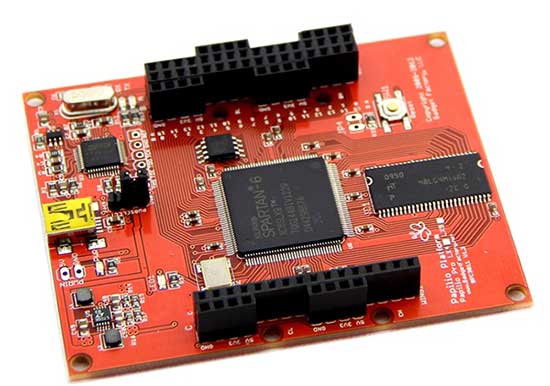
Figure 1: Papilio Pro FPGA development board from the Xilinx Spartan 6 family
Flash-based FPGA boards – These FPGA boards have dedicated flash memory to store configuration data. They do not have SRAM or any volatile memory. These boards are different from SRAM-based FPGA with internal flash. In SRAM-based FPGA with internal flash, configuration data is loaded at boot into internal memory. In Flash-based FPGA, configuration data remains in internal flash memory and is not lost upon power off. These boards are also power efficient compared to SRAM-based FPGA. Some of the popular Flash-based FPGAs include Actel's Igloo and ProASIC3 boards.
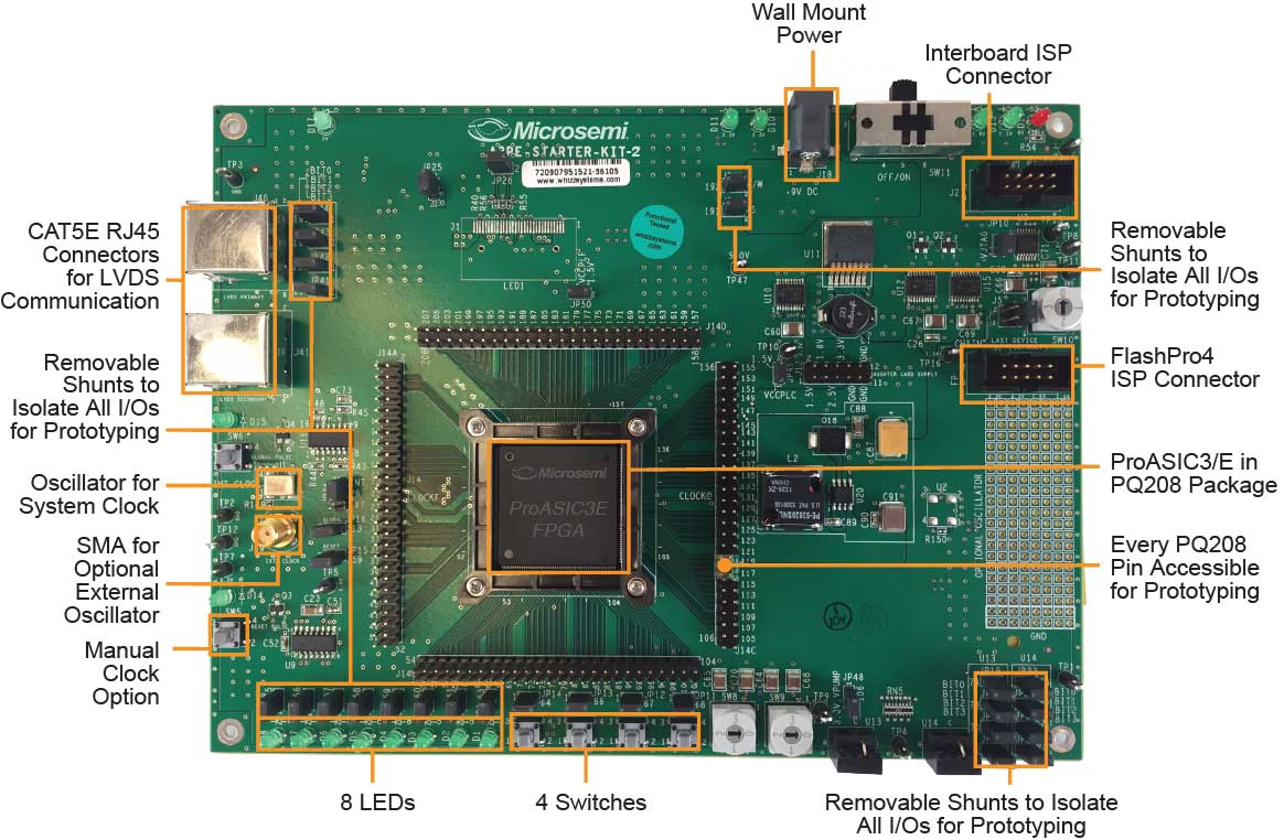
Figure 2: ProASIC3 Flash-Based FPGA Development Board from Actel
Anti-fuse based FPGA boards – These FPGA boards contain anti-fuses that can be blown to conduct current. Once the antifuse is blown, it cannot be changed. Therefore, these FPGA boards are one-time programmable and cannot be reused. Actel's Accelerator is a good example of Anti-Fuse based FPGA boards.
To start development, a SRAM-based FPGA (such as Papilio Pro) or a Flash-based FPGA (such as ProASIC3) should be preferred. Papilio Pro is a popular commonly used FPGA board. It costs around $75 and is easily available. The Papilio Pro operates on 3.3V, so it may require a logic converter to interface with 5V devices. It has 48 I/O pins and comes with a USB port and an integrated FTDI converter for interfacing with a computer.
Configuring the development environment –
Each FPGA board requires its own set of development tools, which are usually freely available from your vendor. As for development in Papilio Pro, Gadget Factory's Papilio loader and Xilinx's ISE Design Suite are the necessary development tools. To download the ISE Design Suite it is necessary to create an account on the Xilinx website. Account creation and download can be done free of charge. The download is a trial version that is free to use for a period of time only. The development environment may be a few GB in size, so it may take some time to download it.
Starting Verilog style –
Once the development tools are installed, you can start coding with VHDL. You can create a new project in Project Navigator and specify the location and working directory. You then need to specify the product details in the project settings. Thus, Papilio Pro belongs to the Spartan 6 family and has a specific device name and package name. These specifications can be checked in the board's official documentation or examined on the chip label. Programming language selection must be Verilog. The next step is to add the source code.
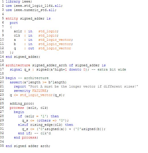
Figure 3: Typical VHDL source code
The source code is compiled into two files – one is the Verilog code with .V extension and the other is the user constraints file with .ucf extension. Verilog code uses labels to specify I/O connections and wire connections to specify hardware connections between logic blocks. The UCF file contains information about the specific chip and various parameters and restrictions.
To add source code, 'New Source' needs to be selected from the Project menu and the file type for the new source needs to be selected 'Verilog Module'. To add the UCF file, 'New Source' needs to be selected from the Project menu and the file type for the new source needs to be selected 'Implementation Constraints File'. After creating the source code and UCF file, the configuration file with .bit extension can be created by double-clicking on “Generate programming file”. The programming file can be opened in Papilio Loader. Now the FPGA board can be connected to the PC and the programming file can be loaded onto the board using Papilio Loader. As the programming file is written to the board, the board starts operating accordingly.
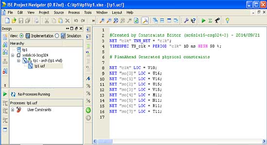
Figure 4: ISE Project Browser
So, grab a development board like Papilio Pro and set up the development environment. Additional components may be required for different applications. So, collect the components, connect them to the I/O header, and start with various Verilog code experiments.