In the previous project, an adjustable power supply circuit was designed with an output voltage in the range between 0V and 30V with a maximum current capacity of 2A. Oftentimes, the required DC power must have both positive and negative voltages. In the previous design, negative voltage could be supplied to a device just by manually reversing the terminal connections. The circuit will input 220V-230V AC and generate a variable DC voltage in the range of +/- 1.25V to +/- 22V at the output. This power supply can provide a maximum current of 1A at the output. To make an adjustable power supply that has negative and positive voltages, a center strip transformer needs to be employed in the circuit design.
In this project, an adjustable regulated positive and negative symmetrical power supply is designed. To reduce any fluctuations and ripples in the output, the supply needs to be regulated so that it can provide a constant voltage at the output. Again, as with the previous design, the voltage is adjusted using a variable resistor. This power supply provides regulated and adjustable voltage at the output.
Designing a power supply circuit is a step-by-step process that involves reducing AC voltage, converting AC voltage to DC voltage, smoothing DC voltage, compensating transient currents, voltage regulation, voltage variation, and voltage amplification. current and short circuit protection.
Required components –

Fig. 1: List of components required for adjustable power supply from +/- 1.25 V to +/- 22 V 1A
Block diagram –

Fig. 2: Block diagram of adjustable power supply from +/- 1.25 V to +/- 22 V 1A
Circuit Connections –
The circuit is assembled in stages and each stage serves a specific purpose. To step down the 230 V AC, a 24 V – 0 – 24 V transformer is used. The secondary coil of the transformer is connected to a full bridge rectifier. The full bridge rectifier is constructed by connecting four 1N4007 diodes together designated as D1, D2, D3 and D4 in the schematics. The cathode of D1 and the anode of D2 are connected to one of the secondary coils and cathode of D4 and the anode of D3 is connected to the other end of the secondary coil. The cathodes of D2 and D3 are connected, of which one terminal is taken from the output of the rectifier and the anodes of D1 and D4 are connected, of which another terminal is taken from the output of the full-wave rectifier. A wire is pulled from the center strip of the transformer that serves as ground for the positive and negative DC outputs.
100 uF capacitors (shown as C1 and C2 in the schematics) are connected between the output terminals of the full-wave rectifier and the center strip of the transformer for smoothing purposes. For voltage regulation, LM317T and LM337 are connected in parallel to the smoothing capacitor. Variable resistors are connected in series to the voltage regulator ICs for voltage adjustment and 10 uF capacitors (shown as C5 and C6 in the schematics) are connected in parallel at the output to compensate transient currents. There are two diodes connected between the input voltage and output voltage terminals of the voltage regulator ICs for short circuit protection.
Get the schematic diagram drawn or printed on paper and make each connection carefully. Only after checking each connection made correctly, connect the power circuit to an AC source.
How the project works –
The power circuit operates in well-defined stages, each stage serving a specific purpose. The circuit operates in the following steps –
1. AC to AC Conversion
2. AC to DC Conversion – Full Wave Rectification
3. Smoothing
4. Transient Current Compensation
5. Voltage regulation
6. Voltage adjustment
7. Short circuit protection
AC to AC Conversion
The voltage of the main sources (electricity fed by the intermediate transformer after reducing the line voltage of the generating station) is approximately 220-230 Vac, which needs to be further reduced to the 24 V level. To reduce 220 Vac to 24 Vac , a step-down transformer with center strip is used. The use of center tapped transformer is to generate positive and negative voltage at the input. The center strip will provide ground to the circuit and the remaining two terminals will provide positive and negative voltage.
The circuit experiences some drop in output voltage due to resistive loss. Therefore, a transformer with a high voltage rating greater than the required 22 V needs to be used. The transformer must provide 1A current at the output. The most suitable step-down transformer that meets the mentioned voltage and current requirements is 24V-0-2 4V/2A. This transformer reduces the main line voltage to +/- 24 Vac, as shown in the image below.

Fig. 3: 24-0-24V Transformer Circuit Diagram
AC to DC Conversion – Full Wave Rectification
The reduced AC voltage needs to be converted to DC voltage through rectification. Rectification is the process of converting AC voltage to DC voltage. There are two ways to convert an AC signal to DC. One is half-wave rectification and the other is full-wave rectification. In this circuit, a full wave bridge rectifier is used to convert 48V AC to 48V DC. Full-wave rectification is more efficient than half-wave rectification as it provides full use of both the negative and positive sides of the AC signal. In the full-wave bridge rectifier configuration, four diodes are connected in such a way that current flows through them in only one direction, resulting in a DC signal at the output. During full-wave rectification, two diodes are forward biased and two other diodes are reverse biased.

Fig. 4: Full Wave Rectifier Circuit Diagram
During the positive half cycle of the supply, diodes D2 and D4 conduct in series while diodes D1 and D3 are reverse biased and current flows through the output terminal passing through D2, output terminal and D4. During the negative half cycle of the supply, diodes D1 and D3 conduct in series, but diodes D1 and D2 are reverse biased and current flows through D3, output terminal and D1. The direction of current in both directions through the output terminal in both conditions remains the same.

Fig. 5: Circuit Diagram showing the positive cycle of the Full Wave Rectifier

Fig. 6: Circuit diagram showing negative cycle of full wave rectifier
1N4007 diodes are chosen to build the full wave rectifier because they have maximum (average) forward current of 1A and in reverse bias condition can sustain peak reverse voltage up to 1000V. This is why 1N4007 diodes are used in this design for full wave rectification.
Smoothing
As the name suggests, it is the process of smoothing or filtering the DC signal using a capacitor. The output of the full wave rectifier is not a constant DC voltage. The rectifier output has twice the frequency of the main sources, but still contains ripples. Therefore, it needs to be smoothed out by connecting capacitors (shown as C1 and C2 in the schematics) in parallel to the output of the full-wave rectifier. The capacitor charges and discharges during a cycle, providing a constant DC voltage as output. Thus, capacitors (shown as C1 and C2 in the schematics) of high value are connected to the output of the rectifier circuit. These capacitors act as filtering capacitors that shunt all the AC through them to ground. At the output, the remaining average DC voltage is smoother and ripple-free.
Capacitors C3 and C4 are connected with adjustment pin. These capacitors prevent the ripple from being amplified as the output voltage increases.

Fig. 7: Smoothing Capacitor Circuit Diagram
Compensating Transient Currents
At the output terminals of the power circuit, capacitors C5, C6, C7 and C8 are connected in parallel to the output terminals. Capacitors C5 and C6 assist in quick response to load transients. Whenever the current of the output loads changes, there is an initial shortage of current, which can be met by this output capacitor.
Capacitors C7 and C8 are ceramic capacitors, the impedance or ESR of ceramic is low compared to an electrolytic capacitor. Therefore C7 and C8 are used in parallel with the electrolytic capacitor just to decrease the equivalent output impedance.
The output current variation can be calculated by
Output current, Iout = C (dV/dt) where
dV = Maximum allowable voltage deviation
dt = transient response time
Considering dv = 100mV
dt = 100us
In this circuit a 1 uF capacitor is used so,
C = 1uF
Iout = 1u (0.1/100u)
Iout = 1mA
In this way it can be concluded that the output capacitor will respond to a current change of 1mA for a transient response time of 100 us.

Fig. 8: Circuit diagram of transient current compensator
Voltage regulation
The power supply circuit must provide regulated and constant voltage, without any fluctuation or variation. For voltage regulation, a linear regulator is required in the circuit. The purpose of using this regulator is to maintain a constant voltage at a desired level at the output. To supply IC LM317 regulated from 1.25V to 22V is used and for -1.25 to -22V at output IC LM337 is used. Both IC are capable of delivering a current of 1.5A, so they are suitable for 1A current requirement. In this circuit, LM317 and LM337 will provide an adjustable voltage corresponding to their input voltage. Both ICs are capable of regulating the load. They will provide regulated and stabilized voltage at the output regardless of fluctuation in input voltage and load current.
LM317 is a positive voltage regulator that provides output in the range of 1.25V to 37V with input voltage up to 40V. Unlike the LM317, the LM337 is a negative voltage regulator that provides -1.25V to -37V with input voltage up to -40V. At the output, both can supply a maximum current of 1.5A according to the technical data sheet under ideal conditions.
To define the desired voltage at the output, a resistive voltage divider circuit is used between the output pin and ground (central strip of the transformer). The voltage divider circuit has a programming resistor (fixed resistor) and another variable resistor. By taking a perfect relationship between the feedback resistor (fixed resistor) and a variable resistor, the desired value of the output voltage corresponding to the input voltage can be obtained. In this circuit, resistors R1 and R2 are used as programming resistance for 317 and 337 respectively. Variable resistors RV1 and RV2 are used to vary the output voltage by 317 and 337 respectively.
The LM317 has the following tolerable power dissipation internally –
Pout = (Maximum IC operating temperature)/ (Thermal Resistance, Junction-Environment + Thermal Resistance, Junction-Enclosure)
Pout = (150) / (65+5) (values according to technical data sheet)
Pout = 2W
Likewise, the LM337 has the following tolerable power dissipation internally –
Pout = (Maximum IC operating temperature)/ (Thermal Resistance, Junction-Environment + Thermal Resistance, Junction-Enclosure)
Pout = (125) / (70+3) (values according to technical data sheet)
Pout = 1.7W
Therefore, 317 and 337 internally can sustain up to 2W and 1.7W of power dissipation respectively. Above 2W and 1.7W, the ICs will not tolerate the amount of heat generated and will start to burn. This can also cause a serious fire hazard. Therefore, heat sinks are needed to dissipate excessive heat from the ICs.
Voltage adjustment
The output voltage can be varied using the tuning pin of ICs 317 and 337. The variable resistors RV1 and RV2 provide the output voltage from 1.25 V to 22 V and -1.25 to -22 V respectively.
Short circuit protection
A diode D5 is connected between the voltage input and voltage output terminals of the 317 IC to prevent the external capacitor from discharging through the IC during an input short circuit. When the input is shorted, the cathode of the diode is at ground potential. The anode terminal of the diode is at high voltage as C5 is fully charged. Therefore, in this case, the diode is forward biased and all the capacitor discharge current passes through the diode to ground. This saves IC LM317 from reverse current.
In a similar way, a diode D6 is connected between the voltage input and output terminals of the 337 IC to prevent the IC from discharging the capacitor C6 across the IC when the input is shorted.

Fig. 9: Short circuit protection circuit diagram
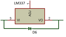
Figure 10:
Tests and precautions
The following precautions must be taken when assembling the circuit:
• The rated current of the step-down transformer, bridge diodes and voltage regulator ICs must be greater than or equal to the current required at the output. Otherwise, it will not be able to provide the required current at the output.
• The rated voltage of the step-down transformer must be greater than the maximum required output voltage. This is due to the fact that ICs 317 and 337 suffer a voltage drop of around 2 to 3 V. Therefore, the input voltage must be 2V to 3V greater than the maximum output voltage and must be at the limit of the input voltages of the LM317 and LM337.
• Capacitors used in the circuit must have a higher voltage rating than the input voltage. Otherwise, the capacitors will start leaking current due to excess voltage on their plates and will explode.
• A capacitor must be used at the output of the rectifier so that it can deal with unwanted noise from the mains. Likewise, the use of a capacitor at the output of the regulator is recommended to deal with rapid transient changes and noise at the output. The value of the output capacitor depends on the voltage deviation, current variations and the transient response time of the capacitor.
• A protection diode should always be used when using a capacitor after a voltage regulator IC, to prevent the IC from countercurrent during capacitor discharge.
• For high output load activation, a heat sink must be mounted in the regulator holes. This will prevent the IC from exploding due to heat dissipation.
• As regulator ICs can only draw current up to 1A, a 1A fuse needs to be connected. This fuse will limit the current in the regulator to 1A. For currents above 1A, the fuse will blow and this will cut off the input power to the circuit. This will protect the circuit and regulator ICs from currents greater than 1A.
Once the circuit is assembled, it's time to test it. Connect the circuit to the main sources and change the variable resistance. Take voltage and current readings at the output terminal of the power circuit using a multimeter. Then connect fixed resistors as load and check voltage and current readings again.
On the LM317 side of the circuit, the input voltage was 24V and when adjusting the variable resistance, the output voltage was between 1.25 to 22V when no load was connected.
When a load is connected to the output the maximum voltage is read as 20V. With a 50Ω resistance load, the output voltage reads at 16 V, showing a voltage drop of 4 V. The output current is measured at 300 mA, so the power dissipation in the 50Ω resistance load is Following:
Pout = (Vin – Vout)*Iout
Pout = (24-16) *(0.3)
Pout = 2.4W
On the LM337 side of the circuit, the input voltage was -24V and when adjusting the variable resistance, the output voltage was between -1.25 to -22V when no load was connected.
When a load is connected to the output, the maximum voltage is read as -20V. With a 50Ω resistance load, the output voltage reads at 17.5 V, showing a voltage drop of 2.5 V. The output current is measured at 320 mA, so the power dissipation in the resistance load 50Ω is as follows:
Pout = (Vin – Vout)*Iout
Pout = (-24 – (-17.5)) *(0.32) (energy dissipation cannot be negative)
Pout = 2.08W
During circuit testing, it was analyzed that when the current demand increases at the output, the output voltage begins to decrease. As current demand increases, the 317 and 337 ICs begin to heat up and the ICs experience more sags, which reduces the output voltages. From the above practical experience, the power dissipation in both ICs is greater than their internal tolerable limits. Therefore, it is recommended to use heat sinks to help cool the ICs and increase the useful life of these voltage regulator ICs.
The power circuit designed in this project can be used as a power adapter for electronic devices and can be used with chipsets that require negative power supply. The circuit can be used to power electronic components such as OP-AMPS, bipolar amplifiers and constant current regulators.
Circuit diagrams
| Circuit Diagram-Adjustable-1.25V-22V-1A-Power Supply | 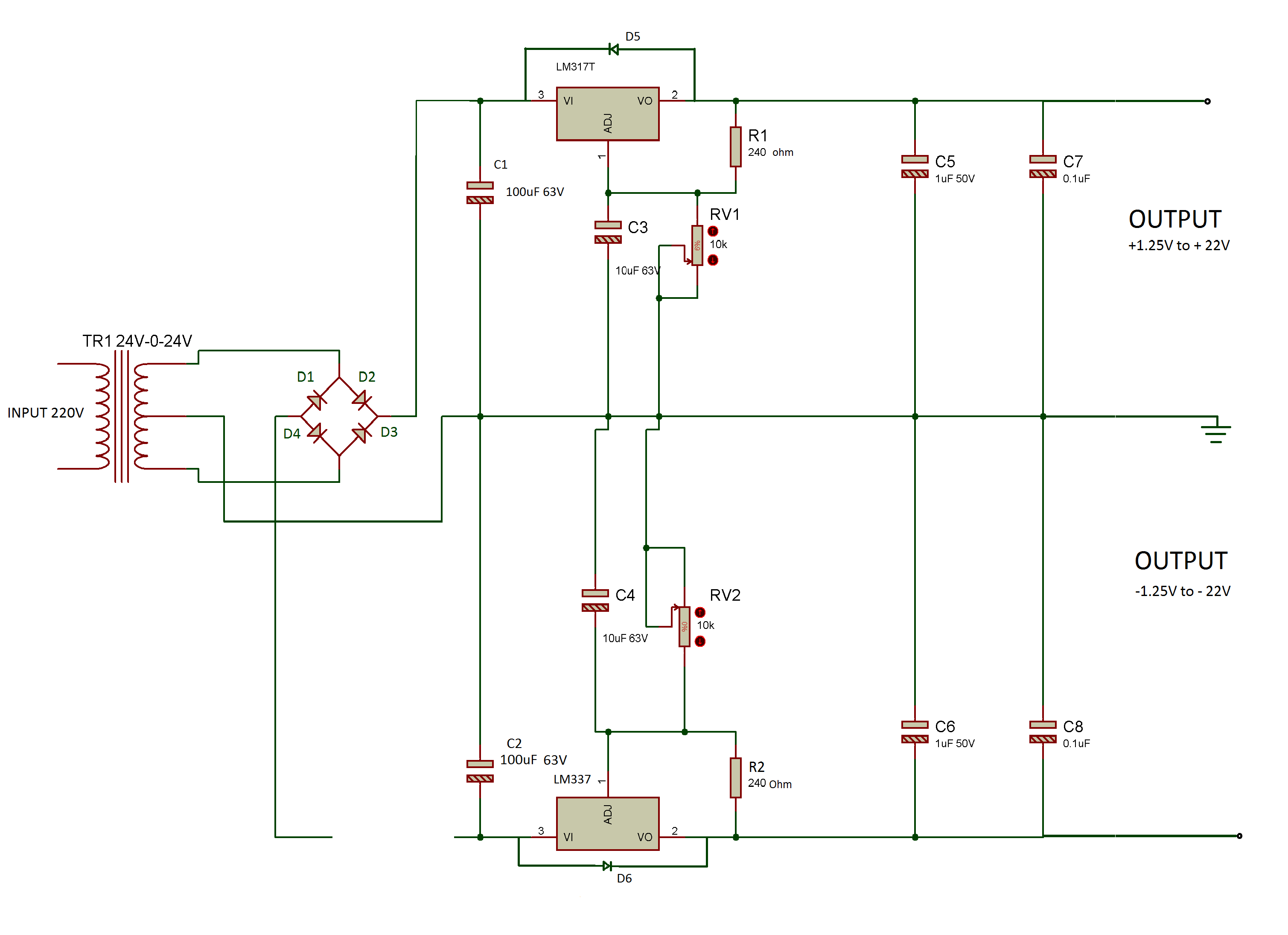 |
Project video