According to The World Semiconductor Trade Statistics (WSTS) – a non-profit organization of semiconductor products companies and source of industry statistics – the electronic design automation (EDA) market was valued at US$11.57 billion in 2020 and is expected to reach US$21.36 billion by 2026. .
EDA refers to the use of computer-aided tools and services for the design, manufacturing, verification and performance testing of highly complex electronic systems – including semiconductor chips, printed circuit boards, multichip modules and microprocessors.
Interestingly, WSTS found that the integrated circuit (IC) semiconductor market was worth $347.63 billion in 2020, and that number is expected to increase.
EDA tools ensure reliable, efficient and (often) reusable electronic chips and circuit boards with guaranteed performance. In this article, we will explore the importance of electronics design automation and review the most popular EDA tools among engineers.
What is EDA?
EDA involves a specific category of hardware, software, processes and services that use computer-related design to develop sophisticated and highly complex electronic systems. As mentioned, these include integrated circuits, printed circuit boards, multichip modules, and microprocessors.
EDA tools are useful for automating, standardizing, and verifying semiconductor and circuit board designs. Tools have become essential due to today's advanced and intricate chips and circuits. The use of computer-aided tools also supports the development of reusable designs, leading to faster manufacturing of ICs and printed circuit boards.
Although semiconductor companies produce integrated circuits, the EDA industry plays a critical role in this production. EDA tools are involved in three main ways. They are used to:
1. Design and validate chip circuits to ensure desired density without compromising performance. Without these tools, it would likely be impossible to achieve the ideal semiconductor designs we see today. Typically, this category of tool design is called Technology Computer-Aided Designs (TCAD).
2. Check designs, ensuring they meet manufacturing requirements. The smallest discrepancies in semiconductor designs can potentially lead to significant chip failures or malfunctions. These tools are considered Design For Manufacturability (DFM). DFM tooling specifically refers to manufacturing reliable and reusable IC designs with high packaging density.
3. Monitor the performance of semiconductor projects throughout their life cycle. Different tools evaluate projects depending on the production stage, from post-manufacturing to final deployment. These EDA tools are categorized as Silicon Lifecycle Management (SLM).
Each EDA tool involved in IC manufacturing falls into one of three categories: TCAD, DFM, or SLM.
For circuit boards, EDA tools are used for computer-supported layout design and automation control for PCB manufacturing. A slightly more recent area of tool use is Semiconductor Intellectual Property (IP).
Semiconductor IP provides pre-engineered circuits that can be integrated as-is into a variety of applications. This segment focuses on semiconductor designs that can be frequently reused and easily adapted for diverse use cases. This provides rapid development and updating of electronic systems.
Why is EDA important?
Very large scale integration (VLSI) and ultra large scale integration (ULSI) have become the semiconductor industry standards. With such high levels of packaging density – where millions of transistors, diodes and components are integrated into a small chip – a small failure can lead to complete dysfunction.
EDA tools allow developers to design, simulate, model, validate, verify, and analyze circuit designs to detect potential problems before production. They also enable maintenance and reuse of designs so they can be easily adapted to other applications (such as Semiconductor IP). Furthermore, the tools contribute to improved projects over time.
In the future, expect denser designs with greater complexities, which means EDA tools will become even more evolved and used in the semiconductor and PCB industries.
EDA Applications
EDA is a software industry that works closely with semiconductor and PCB manufacturers. Industries using embedded systems, mechatronics and photonics also rely heavily on EDA tools. These tools are widely used by users of technology verticals such as aerospace, automotive, biomedical, telecommunications, cybersecurity, machine learning, cloud computing, consumer, edge computing, internet of things, and automation.
Essentially, EDA tools have become essential for the development, automation and testing of electronic system designs, whether these systems are semiconductor chips, multichip modules or printed circuit boards.
How EDA works
EDA tools are an integral part of the infrastructure for designing and developing electronic systems. They are typically used to:
Simulation: Simulation tools provide a description of a proposed circuit and predict its behavior before implementation. The description is done with the help of a standard hardware description language such as VHDL or Verilog.
Simulation tools model the circuit behavior of individual components under different conditions and predict how they would behave when integrated into a circuit. Based on the operation of the components, these tools predict the overall functioning of the circuit design while detecting potential faults.
For highly compressed designs, such as graphics processors or NPUs, simulation tools may also require hardware assistance. These tools are useful for logic simulation, transistor-level simulation, CAD technology, and hardware emulation.
Design: Design tools introduce the proposed circuit function, supporting its implementation through the assembly of circuit components. These tools are useful for automating circuit production and validating designs before production. They typically interconnect elements at the logical and physical levels.
The interconnection of circuit elements at the logical level is a logical synthesis. This may involve high-level synthesis where HDL is converted to the register transfer level.
Additionally, design tools are used for the physical layout or actual location and routing of components on a silicon wafer or circuit board. They can also provide custom layouts using an iterative process with the circuit designer.
Analysis and verification: Verification tools examine designs at the logical or physical level to find flaws and ensure performance. These tools can be used for physical verification, model verification, functional verification, equivalence verification, static timing analysis, and CDC verification.
Due to the complexity of VLSI designs, verification often involves tens of thousands of rules.
- During physical verification, interlocking geometries are examined to ensure they are placed in accordance with the foundry's manufacturing requirements.
- During functional verification, the simulation compares what is expected with the actual behavior of the circuit design.
- During equivalence checking, the behavior of a circuit design is algorithmically verified without any input simulation.
EDA tools are also used for mask data preparation during semiconductor chip manufacturing and post-production functional safety analysis.
The role of EDA tools is significant because they are involved in the entire life cycle of a chip or circuit, from planning, design, implementation, manufacturing and testing.
Top EDA Tools
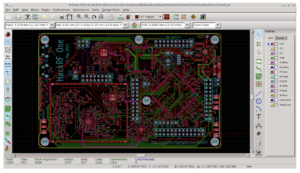
Some of the top EDA tools used in PCB design and manufacturing include Eagle, KiCAD, Multisim, LibrePCB, gEDA, Fritzing, Pulsonic, Altium, OrCAD, Upverter, EasyEDA, Pathwave Advanced Design System, Pcb-rnd, QUCS, Electric, and Xcircuit.
Some of the top EDA tools used in chip design and development include Primetime, Innovus, Caliber, Pathwave, Magic, IDesignSpec, IVerifySpec, Active-HDL, Visula, Electric VLSI Design System, Xilinx Vivado, SmartSim, and Verilator.