In electronic circuits, the common collector configuration is a central building block with unique application possibilities, special properties, and a series of optimization strategies. Its importance can be felt in several areas of electronics as a versatile arrangement for amplification, signal buffering and impedance matching. This exploration delves deep into the common collector configuration, decoding how it works and illuminating its real-world applications. From understanding their non-inverting properties to optimizing their performance, this journey promises to demystify configuration and provide insights that bridge theory and practical circuit design.
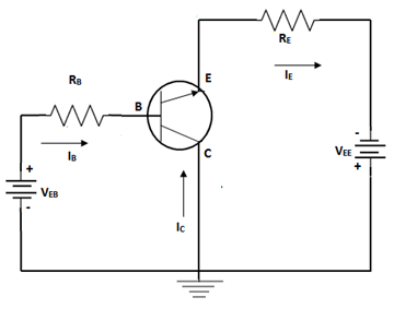
Common collector structure of an NPN transistor

Transistor circuit configuration
Transistors are essential components of modern electronics and serve as amplifiers, switches and signal processors. However, in real-world scenarios, transistors are not ideal devices and can exhibit certain non-ideal behaviors. One of these behaviors is known as “leakage current”.
Leakage currents are small, unintended currents that flow between different transistor terminals, even when they are turned off or no external input is applied. These currents are the result of various physical phenomena in the semiconductor materials and the internal structure of the transistor.
There are basically two types of leakage current in transistors:
Collector current leak (ICEO or ICO)
In a bipolar transistor (BJT), a small leakage current, called collector reverse current (ICEO for NPN transistors or ICO for PNP transistors), flows between the collector and emitter when the transistor is in the off or reverse-biased state. This happens due to minority charge carriers (holes in NPN, electrons in PNP) that are present in the base region and can diffuse through the collector-base junction with reverse bias.
Base Current Leakage (IBO)
Even when a transistor is turned off, there may be a small base current loss (IBO) between the base and emitter terminals. This loss is mainly due to the reverse-biased base-emitter junction, which allows a small number of minority carriers to pass around the corner.
Leakage currents can have several effects on circuit design and performance:
energy consumption
Although leakage currents are typically very small, in high-density integrated circuits such as those found in modern microprocessors, the cumulative effect of leakage currents across multiple transistors can result in significant power consumption, even when a device is intended to operate at low power. mode.
Signal Integrity
In certain applications where transistors amplify weak signals, leakage currents can introduce errors or distortions into the amplified signal, compromising signal integrity.
Heat generation
Although the leakage currents are small individually, they can contribute overall to the development of heat in the transistor. In high-performance devices, controlling this heat is critical to ensuring reliable operation.
To mitigate the effects of leakage current, circuit designers use techniques such as transistor sizing, biasing, and advanced process technologies that minimize the effects of leakage current. Leakage current continues to be a topic of research and discussion in semiconductor device manufacturing and circuit design to create more efficient and reliable electronic systems.
Current Gain Factor
Relationship between γ and α
Relationship between transistor currents
-
I C =β.I b = α.I b = (β / (1+β)).I E
-
I b = I C /β = I E /(1+β) = (1-α).I E
-
I E = I C /α = ((1+β) / β).I C = (1+β).I b = I b .(1-α)
Explanation of Thevenin's Theorem
Thévenin's theorem is a fundamental concept in the analysis of electrical circuits that simplifies complex linear circuits into simpler equivalent circuits. It states that any two-terminal linear network with resistors and independent sources of voltage or current can be replaced by an equivalent circuit consisting of a single voltage source in series with a single resistor. This simplified circuit is called a Thévenin equivalent circuit.
The phrase is named after the French engineer Léon Charles Thévenin, who introduced it in the late 19th century. Thevenin equivalent allows engineers to analyze and solve complex circuits more easily, especially in network analysis, circuit design, and troubleshooting.
This is how Thévenin's theorem works
Find the Thévenin voltage (Vth)
To determine the Thevenin equivalent voltage (Vth), the circuit voltage is calculated at terminals A and B when the load (resistor or other components) is disconnected. This can be done using node, mesh or any other suitable circuit analysis method.
Find the Thévenin resistance (Rth)
The Thevenin equivalent resistance (Rth) is calculated by temporarily removing all voltage and current sources from the circuit. A test voltage source is then applied to connections A and B and the resulting current is calculated. Rth is equal to the ratio of test voltage to calculated current.
Build the Thevenin equivalent circuit: Once Vth and Rth are determined, the Thevenin equivalent circuit is constructed by placing a voltage source (Vth) in series with a resistor (Rth) between terminals A and B.
The Thevenin equivalent circuit simplifies circuit analysis in several ways:
- Simplification: Complex networks with multiple components can be reduced to a single voltage source and resistor, greatly simplifying calculations.
- Load analysis: Thévenin's theorem can be used to analyze how the circuit responds to different loads connected between terminals A and B.
- Network equivalence: The theorem establishes the concept of electrical equivalence, in which a complex circuit can be replaced by a simpler one that presents the same behavior at the relevant terminals.
- Maximum power transmission: Thevenin's theorem is often used to determine the load resistance that maximizes power transfer from source to load.
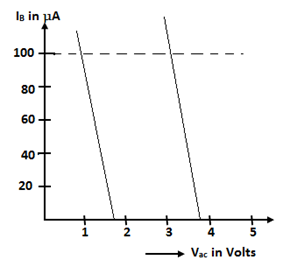
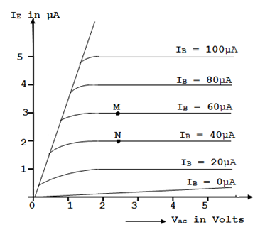
Common Collector Configuration: I/O Properties

Transistor Leakage Currents
Transistor leakage current is a significant problem in modern semiconductor devices and integrated circuits. These small, unintended currents can significantly impact the performance, energy efficiency, and reliability of electronic systems. Leakage currents arise due to the incomplete isolation of various regions of the transistor and the inherent physical properties of semiconductors.
There are basically two types of transistor leakage current:
Subthreshold leakage current (out-of-state leakage current)
This type of leakage current occurs when a transistor is turned off, meaning it should not conduct any current. However, due to the nature of semiconductor materials and the quantum mechanical phenomena that occur, a small current, the so-called subthreshold leakage current, can flow between the transistor connections. This current becomes more significant as transistors get smaller and operate at lower supply voltages. Sub-threshold leakage current is a significant factor in the power consumption of modern integrated circuits, especially in standby or power-saving modes.
Leak at the gate
Gate leakage current is the current that flows through the insulating oxide layer between the gate and channel of a transistor when it should not be conducting. In MOSFETs (metal-oxide semiconductor field-effect transistors), this can occur due to tunneling of electrons through the thin-gate oxide. As transistor dimensions continue to decrease, the gate oxide thickness also decreases, making gate leakage current more pronounced and problematic. Techniques such as high-k dielectrics reduce gate leakage current in advanced semiconductor processes.
Leakage currents can lead to several challenges:
- Energy efficiency: Excessive leakage currents can result in higher power consumption, shorten the battery life of portable devices, and increase heat generated in integrated circuits.
- Signal Integrity: Leakage currents can affect the accuracy and integrity of signals and impact the performance of analog and mixed-signal circuits.
- Reliability: Over time, leakage currents can cause device aging, which in turn can lead to potential failures and reduced lifespan of electronic components.
To solve these problems, semiconductor manufacturers and developers use a number of strategies:
- Optimized process: Advanced manufacturing processes and materials are being developed to reduce transistor leakage currents.
- Transistor design: Transistor architectures are modified to minimize leakage currents without sacrificing performance.
- Power Limiting: To avoid power consumption due to leaks, unused circuit blocks are completely turned off when not in use.
- Dynamic Voltage and Frequency Scaling: Voltage and frequency are dynamically adjusted based on workload to reduce power consumption during periods of low activity.
- Leakage-aware design: Circuit designers use specialized tools to account for leakage currents during the design phase and implement strategies to mitigate their impact.
Collector-to-base leakage current (I CBO )
-
When the emitter is open and the collector-base junction is reverse biased, a small current (collector-base leakage current) flows through the hub.
-
It consists of two components:
-
The temperature-dependent component current due to thermal generation of electron-hole pairs and
-
The voltage-dependent portion of the current is due to surface leakage across the collector-base connection.
-
ICBO represents this. This current is called reverse saturation or reverse collector current and is characterized by I. CEO For silicon transistors, it doubles with every tenth increase in temperature.
Leakage current from collector to emitter (I CEO )
-
When the base is an open circuit and the collector-emitter junction is reverse biased, a small current, called the collector-emitter leakage current, I CEO, flows from the collector to the emitter.
-
This current also depends on the collector temperature and the emitter voltage; you can show it.
Leakage current emitter base (I CEO )
-
When the collector is open and the base-emitter junction is reverse biased, a small current occurs, called base-emitter leakage current I. CEO flows through the intersection.
Transport factor (β)
Conclusion
In conclusion, the study of the common collector configuration provided valuable information about its importance and application in electronic circuits. This versatile transistor configuration provides an effective buffer between high and low impedance lines, amplifying signals with minimal distortion. We decipher its unique properties through detailed analysis such as unity voltage gain and non-inverting properties. We can optimize its use in various electronic projects by understanding the interaction of input and output characteristics. The ability of the common collector configuration to provide high current gain while maintaining phase coherence is invaluable in audio and radio frequency applications. As technology advances, this basic configuration continues to be essential for developing efficient and robust electronic systems.


