The modern world is full of gadgets that get excited when they sense human movement. Automatic doors in elevators and shopping malls, burglar alarms in homes and stores, automatic lighting systems, electronic amenities in bathrooms are just a few examples where human presence or absence puts the device in an active or passive state. Smart, right? Now, what if we say that behind this intelligent response to movement there is a device that doesn't even reach the 2 cm mark in size. Known as a Pyroelectric or Passive Infrared Sensor ( PIR in both cases), this small electronic device is the curious case of this Insight.
Every object that has a temperature above perfect zero emits thermal energy (heat) in the form of radiation. We Homo sapiens radiate at a wavelength of 9 to 10 micrometers throughout the day. The PIR sensors are tuned to detect this IR wavelength that only emanates when a human comes close to them. The term “pyroelectricity” means: heat that generates electricity (here, a small amplitude electrical signal). Since these sensors do not have an infrared source of their own, they are also called passive.
How does PIR Sensor selectively respond to IRs radiated by humans? Up to what range can this sensor work? What is inside this sensor that makes it work? That and answers to more questions in this Insight on PIR sensors. What adds more charm to this Insight is that the 10m Panasonic sensor is also one of the smallest commercially available PIR sensors to date.
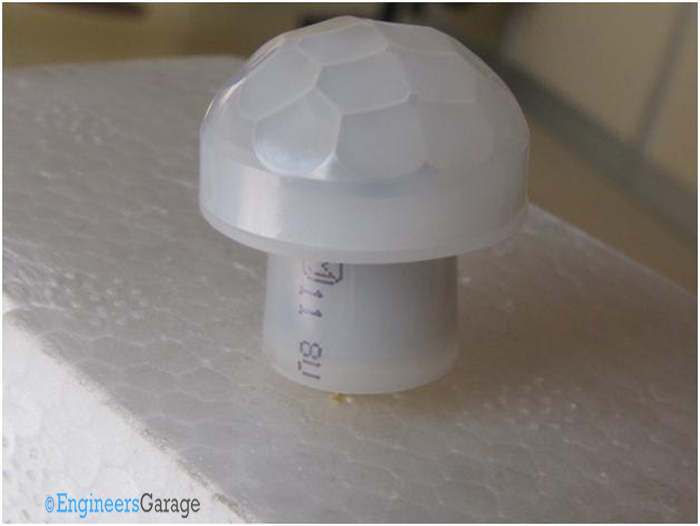
Fig. 1: Image of Panasonic 10mm infrared sensor
Fresnel Lens Array
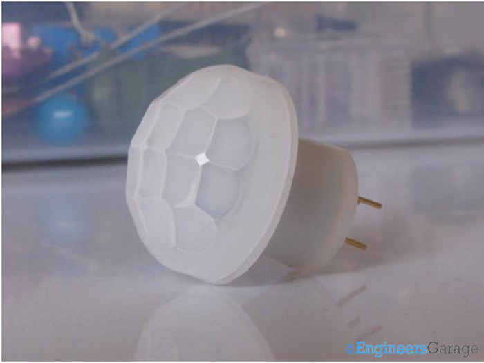
Fig. 2: Image of the sensor's external body
Image 02 shows a Panasonic 10m sensor: the PIR sensor unit enclosed in a plastic chamber. The chamber is translucent, dressed in a honeycomb-like lid, and has an opening at the bottom from which the sensor's solder dip legs protrude.
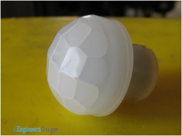
Fig. 3: Image showing the Hive Structure and Curved Segments of the Upper Sensor Region
When looking closely at the upper region of the sensor, the honeycomb-shaped structure, curved segments are seen. These curved segments are Fresnel lenses that constitute an array that increases the sensor's detection zone. The Fresnel lens array is known to capture more infrared radiation and focus it into a relatively smaller spot. Detection is more stable and the maximum detection distance is also increased. The Fresnel lens is designed to be translucent so that it can capture only infrared radiation without getting unwanted radiation from the visible spectrum of light.
The number of Fresnel lenses can vary across the array and this sensor has a total of 20 lenses.
Inside plastic frames
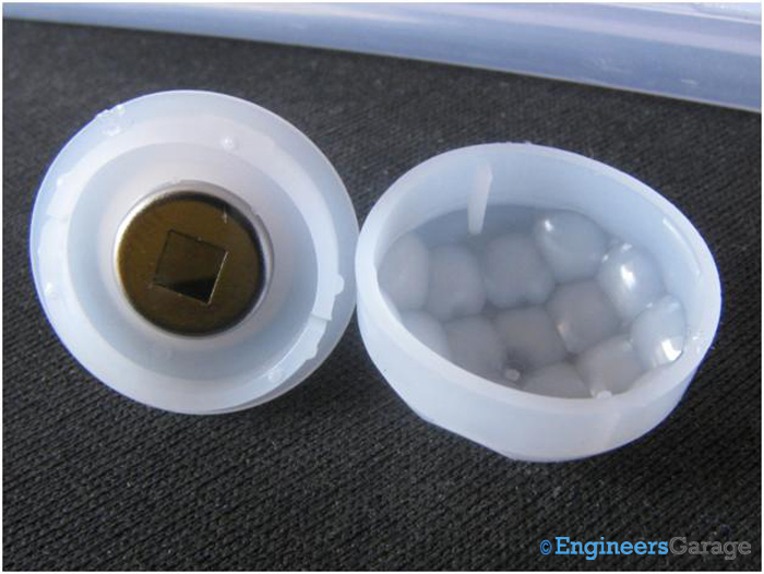
Fig. 4: Internal configuration of the PIR sensor
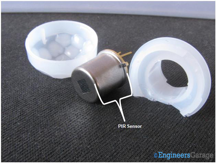
Fig. 5: PIR sensor shape and structure
The lid loaded with Fresnel die is placed firmly over the base region of the plastic molding. There is, however, no locking mechanism to hold it, which makes removing the Fresnel lens assembly from the plastic assembly curious. Below the Fresnel lens assembly is the PIR sensor that is firmly placed in the plastic frames. Sensor placement is crucial as it must receive the maximum amount of infrared radiation coming from the lens array. Therefore, it is placed in the center of the frames where maximum radiation converges to fall.
IR filter and TO5 metal can
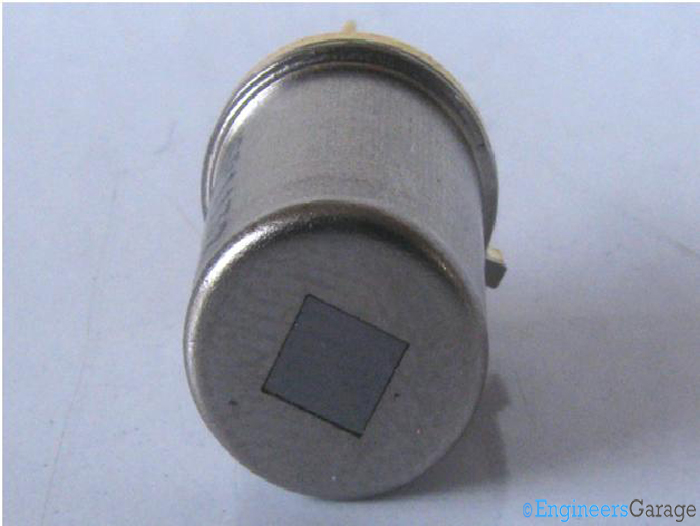
Fig. 6: Sensor infrared filter
| Fig. 6: Se infrared filter |
At the top of the sensor is the infrared filter. Looking more like a square glass, this filter selects the desired wavelength at which the sensor wants to respond. As this sensor was designed to detect human presence, the wavelength chosen is 8 micrometers to 14 micrometers, which is the range within which the human body radiates electromagnetic rays.
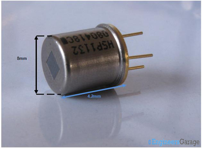
Fig. 7: Sensor design specifications
The sensor body is TO5 metal can structure. TO5 is an industry-based standard used to package various small modules such as transistors, sensors, etc. The TO5 metal casing protects the internal circuit from external influences such as vibrations or noise that could disturb the normal operation of the circuit.
Sensor element and chip
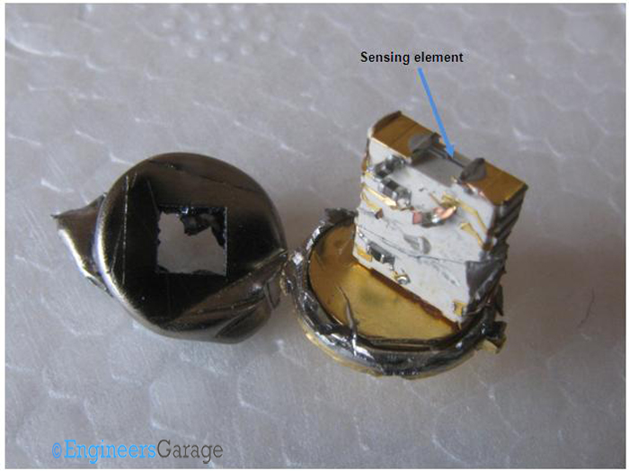
Fig. 8: PIR Sensor PCB
Removing the sensor cover reveals a small PCB that houses the detection module, amplifier and a comparator circuit. Figure 09 shows the upper part of the PCB where the sensing element is placed. Sensing elements are typically made of ferroelectric ceramic (contains lead) or lithium tantalite (lead-free). To increase the signal receptive power, various sensing elements are used. The sensor is of the quadruple type and has 4 sensor elements connected in a matrix.
The IR rays, after passing through the filter, reach this sensing element which generates a charge. The magnitude of the charge produced is directly proportional to the number of rays that fall on the element.
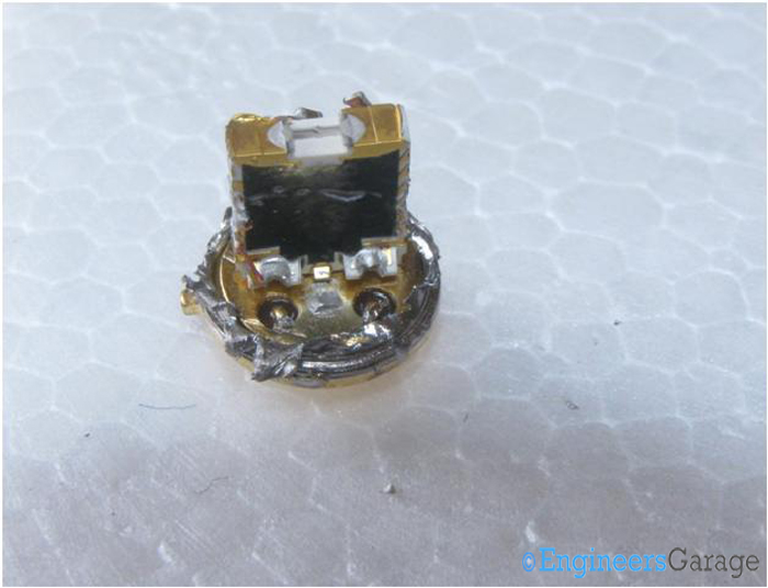
Fig. 9: PCB Amplifier and Comparator
After the charge is developed, it is passed to the amplifier circuit, from which it is transmitted to the comparator. Further embedded in this PCB are the amplifier and comparator. Previously, these two circuits were included in the external circuit; however, including them in the sensor module makes the circuit more compact. As these two circuits are already pre-defined for the IR radiation spectrum, the results tend to be more precise and accurate.
Comparators are used in those sensor modules that provide a digital output, like this one.
FET and Leads
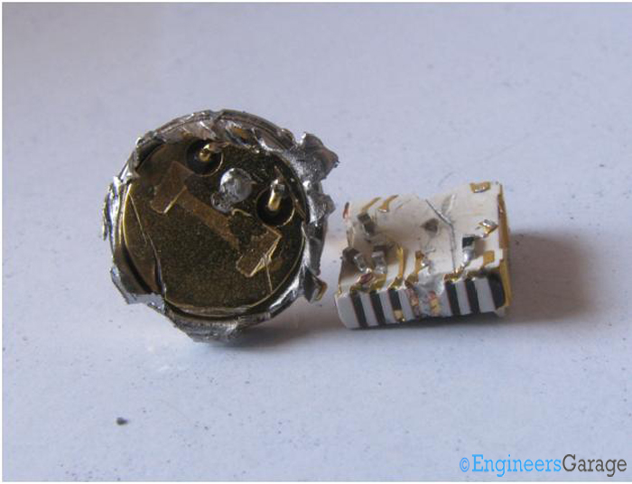
Fig. 10: Base plate and its components
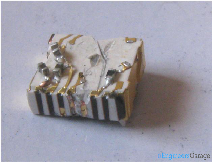
Fig. 11: Processor Unit and Built-in Resistors
The base plate and the rest of the sensor structure is a Field Effect Transistor, FET. Even if the charge produced is amplified, it can still only generate voltages of the order of 1mV. FETs can work at such low voltage and can easily transmit the voltage to the processor unit through which the sensor is connected.
Image 10 details the base board while image 11 shows the processor unit with some resistors.
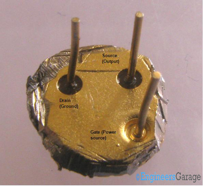
Fig. 12: Multifunctional PIR sensor connection cables
At the bottom of the sensor are, as expected, the connection wires. In this sensor, they multitask: allowing the sensor to be soldered, taking care of small power requirements, and sending output to the processing unit.
Image 12 shows details of the positioning of the connection cables, organized in the same way as in a JFET. The specific function of each electrode is shown in the image.

