In the previous tutorial, gate-level minimization of Boolean functions was discussed. A Boolean function must be expressed in standard form as sum of products (SoP) or product of sums (PoS). Once an in case Boolean function is minimized to SoP or PoS form, it can be easily fabricated as a two-level implementation of AND and OR gates. A two-level implementation is preferred so that there is minimal delay in signal propagation through the logic gates from input to output of the digital circuit.
Practically, digital circuits are built with NAND or NOR gates instead of AND or OR gates. NAND and NOR gates are easy to manufacture with semiconductor components. These are the universal gates from which all other logic gates can be constructed. This is why all digital ICs are built with NAND or NOR gate instead of other logic gates.
NAND as Universal Gate –
NAND is a universal gate. All other logic gates can be constructed by NAND gate. A NOT gate can be constructed by a single-input NAND gate. A single-input NAND gate works the same as inverter or NOT gate. AND gate can be implemented by connecting a NAND gate to a single-input NAND gate, where the single-input NAND gate will function as an inverter or NOT gate. The OR gate can be implemented by connecting inputs to single-input NAND gates acting as an inverter which then connects to a NAND gate. The implementation of AND, OR and NOT gates with the help of NAND gate is shown in the following logic gate diagrams –
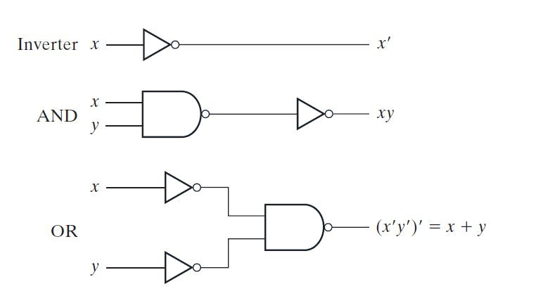
Fig. 1: Image showing the implementation of AND, OR and Invert with NAND Gate
Two-level implementation with NAND Gate –
For two-level implementation of a Boolean function with NAND gate, it must be expressed in the form of sum of products. AND (product) operation between Boolean variables (binary data paths) can be implemented by connecting the inputs to a NAND gate which must be connected to a single input NAND gate acting as an inverter. The OR (sum) operation can be implemented by connecting level 1 outputs to single-input NAND gates acting as inverters that must be connected to a NAND gate. Since the one's complement of a Boolean variable is its normal form, single-input NAND gates at level-1 output and level-2 input on the same lines can be removed. Therefore, a product sum expression can be implemented by NAND gates via a simple NAND-NAND implementation.
Suppose a four-variable Boolean function F is as follows –
F = AB + CD
In AND-OR implementation, your logic gate diagram will be as follows –
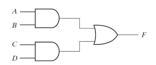
Fig. 2: Image showing the two-level AND-OR implementation before the NAND-NAND implementation
A NAND gate can be shown as AND-Invert or Invert-OR as they are equivalent. The following graphical symbols can be used for NAND gate –

Fig. 3: NAND gate symbols
By replacing the AND plus OR gate with the NAND gate in the F function implementation, the following logic diagram is obtained –
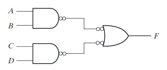
Fig. 4: Image showing the replacement of AND-OR gates by NAND gate
As mentioned above, the one's complement of a Boolean variable is its normal form, single-input NAND gates at level 1 output and level 2 input on the same lines can be removed. Therefore, after removing an even number of inverters in the same row, the final NAND-NAND implementation of the function will be as follows –
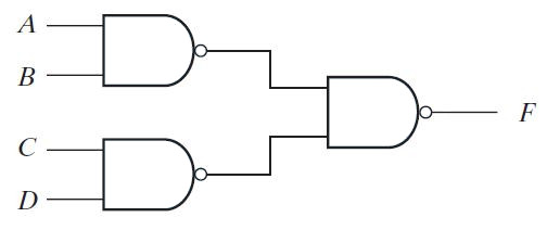
Fig. 5: Image showing the two-level NAND-NAND implementation of a product sum expression
Multilevel implementation with NAND Gate –
The gating structure of a digital circuit does not always need to be viable to be implemented at two levels. Often, due to design limitations or manufacturing feasibility of an IC, it may be necessary to implement the logic gate diagram of a digital circuit at three or four levels. here are also some boolean functions like Ex-OR, which can only be implemented in gate structures of 3 levels or more. In this case, the Boolean function must first be expressed in terms of AND, OR, and NOT gates. A logic gate diagram with AND, OR and NOT gates must be drawn and the AND, OR and NOT gates must be replaced with their NAND equivalents. Now, the even number of bubbles (denoting NOT in NAND gate) in the same rows should be removed and the remaining single bubbles in the rows should be replaced with single-input NAND gates. On the left is the all-NAND logic gate diagram of the digital circuit.
NOR as Universal Gate –
NOR is also a universal gate like NAND gate. All other logic gates can also be constructed by NOR gate. A NOT gate can be constructed by a one-input NOR gate. A single-input NOR gate works in the same way as the inverter or NOT gate. OR gate can be implemented by connecting a NOR gate to a single-input NOR gate, where the single-input NOR gate will function as an inverter or NOT gate. The AND gate can be implemented by connecting inputs to single-input NOR gates acting as an inverter which then connects to a NOR gate. The implementation of other gates with a NOR gate is double the implementation of other gates with a NAND gate. The implementation of AND, OR and NOT gates with the help of NOR gate is shown in the following logic gate diagrams –
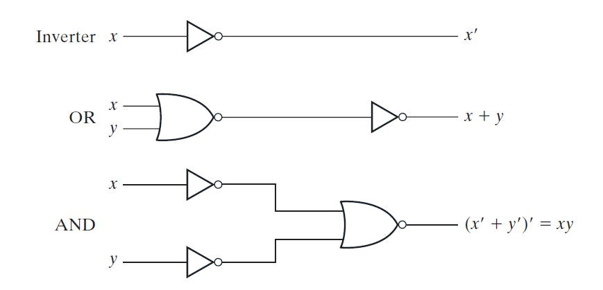
Fig. 6: Image showing the implementation of AND, OR and Invert with NOR gate
Two-level implementation with NOR Gate –
For two-level implementation of a Boolean function with a NOR gate, it must be expressed in the form of a product of sums. The NOR gate implementation of the AND, OR, and NOT gate is just the dual of the NAND gate implementation. OR (sum) operation between Boolean variables (binary data paths) can be implemented by connecting the inputs to a NOR gate which is to be connected to a single input NOR gate acting as an inverter. AND (product) operation can be implemented by connecting level 1 outputs to single-input NOR gates acting as inverters that must be connected to another NOR gate. Since the one's complement of a Boolean variable is its normal form, the single-input NOR gates at the level-1 output and the level-2 input on the same lines can be removed. Therefore, a sum product expression can be implemented by NOR gates via a simple NOR-NOR implementation.
Suppose a four-variable Boolean function F is as follows –
F = (A + B)(C + D)
In AND-OR implementation, your logic gate diagram will be as follows –
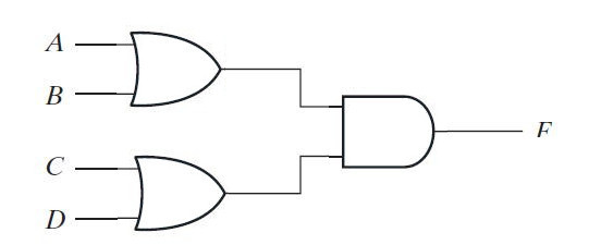
Fig. 7: Image showing the two-level AND-OR implementation before the NOR-NOR implementation
A NOR gate can be shown as OR-Invert or Invert-AND as they are equivalent. The following graphic symbols can be used for NOR gate –

Fig. 8: NOR gate symbols
By replacing the AND, OR and NOT gates with the NOR gate in the implementation of the F function, the following logic diagram is obtained –
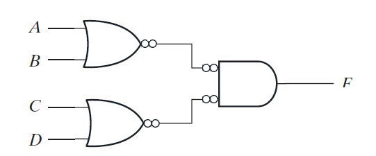
Fig. 9: Image showing the replacement of AND-OR gates by NOR gate
As mentioned above, the one's complement of a Boolean variable is its normal form, the single-input NOR gates at level 1 output and level 2 input on the same lines can be removed. So, after removing an even number of inverters in the same line, the final NOR-NOR implementation of the function will be as follows –
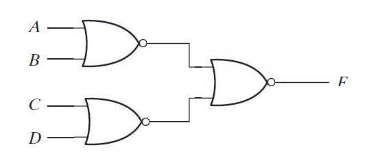
Fig. 10: Image showing the two-level NOR-NOR implementation of a sum expression product
All possible implementations of two levels and non-degenerate forms –
Considering the two-level implementation of Boolean functions and having AND, OR, NAND, and NOR gates available, there can be sixteen possible combinations for two-level implementation of a Boolean expression. The eight of these combinations degenerate into a single operation, which is why they are called degenerate forms. The eight degenerate forms are as follows –
1) EE : Degenerates to AND operation. As if there are four Boolean variables A, B, C and D connected in the AND-AND gate structure, it will be deduced as follows –
F = (AB)(CD)
=ABCD
2) E-NAND : Degenerates to NAND operation. As if there are four Boolean variables A, B, C and D connected in the AND-NAND gate structure, it will be deduced as follows –
F = ((AB)(CD))'
= (AB)' + (CD)'
= A' + B' + C' + D'
= (ABCD)'
3) OR OR : Degenerates to OR operation. As if there are four Boolean variables A, B, C and D connected in the OR-OR gate structure, it will be deduced as follows –
F = (A + B) + (C + D)
= A + B + C + D
4) OR-NOR : Degenerates to NOR operation. As if there are four Boolean variables A, B, C and D connected in the OR-NOR gate structure, it will be deduced as follows –
F = ((A + B) + (C + D))'
= (A + B)'(C + D)'
=A'B'C'D'
= (A + B + C + D)'
5) NAND-OU : Degenerates to NAND operation. As if there are four Boolean variables A, B, C and D connected in the NAND-OR gate structure, it will be deduced as follows –
F = (AB)' + (CD)'
= A' + B' + C' + D'
= (ABCD)'
6) NAND-NOR : Degenerates to AND operation. As if there are four Boolean variables A, B, C and D connected in the NAND-NOR gate structure, it will be deduced as follows –
F = ((AB)' + (CD)')'
= (A' + B' + C' + D')'
= (ABCD)
7) NOR-E : Degenerates to NOR operation. As if there are four Boolean variables A, B, C and D connected in the NOR-AND gate structure, it will be deduced as follows –
F = (A + B)'(C + D)'
=A'B'C'D'
= (A + B + C + D)'
8) NOR-NAND : degenerates to OR operation. As if there are four Boolean variables A, B, C and D connected in the NOR-NAND gate structure, it will be deduced as follows –
F = ((A + B)'(C + D)')'
= (A + B) + (C + D)
= A + B + C + D
The remaining eight forms derive the sum-of-products expression or the sum-product expression for a Boolean function. These are called non-degenerate forms. The eight non-degenerate forms are AND-OR, AND-NOR, OR-AND, OR-NAND, NAND-AND, NAND-NAND, NOR-OR, and NOR-NOR. AND-OR is a dual of OR-AND, NAND-NAND is a dual of NOR-NOR, NOR-OR is a dual of NAND-AND while OR-NAND is a dual of AND-NOR and vice versa. The AND-OR and OR-AND forms are basic forms of a Boolean expression. The NAND-NAND and NOR-NOR forms are the universal implementation of any Boolean function. NAND-AND and AND-NOR are equivalent and called the AND-OR-Invert implementation. OR-AND and NOR-OR are also equivalent and called OR-AND-Invert implementation.
AND-OR-Invert implementation –
Both NAND-AND and AND-NOR perform the AND-OR-Invert operation. It is a simple AND-OR operation with inverted operation implemented at the output. Suppose there are four Boolean variables – A, B, C and D, then the NAND-AND operation between them will be as follows –
F = (AB)'(CD)'
= (AB + CD)'
Similarly, AND-NOR operation with four Boolean variables – A, B, C and D will be deduced as follows –
F = (AB+CD)'
OR-AND-Invert implementation –
Both OR-NAND and NOR-OR perform the OR-AND-Invert operation. It is a simple OR-AND operation with inverted operation implemented at the output. Suppose there are four Boolean variables – A, B, C and D, then the OR-NAND operation between them will be as follows –
F = ((A + B)(C + D))'
Similarly, the NOR-OR operation with four Boolean variables – A, B, C and D will be deduced as follows –
F = (A + B)' + (C + D)'
= ((A + B)(C + D))'
Now, with knowledge of gate-level implementation, any Boolean function can be constructed with universal logic gates – NAND and NOR. In the next tutorial, there is a brief introduction to VHDL . VHDL is a computer-based language that describes the hardware of a digital circuit in textual form. It is a computer-based design tool that is extremely useful in designing large-scale digital circuits. Designing small circuits can be done manually, but large digital circuits require computational tools to design. These tools not only make the design process easier but also reduce the chances of a flawed design.

