Most devices require 5Vs to operate. In this experiment, we will design a DC to DC Buck Converter that provides 5Vs of regulated output. We will use a tunable AP65111AWU-7 switched mode IC for DC voltage conversion and analyze its performance.
IC Specification:
- A reduction from 12V DC to 0.8V to 6V DC
- An output current of 1.5A
- A switching frequency of 500kHz
Note: For more information on DC to DC Buck Converters, see this series on SMPS.
The design
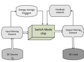
Basic design of the DC-DC converter.
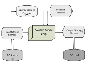
Most switch-mode ICs consist of an oscillator (for frequency generation), a transistor (which acts as a switch), and an error amplifier (to provide voltage regulation). Along with these components, we will need some external components for this project, including:
- An energy storage element – Inductor
- An input/output filtering element – Capacitor
- A feedback network – Voltage divider network to set fixed output voltage
Principle
An inductor stores energy in the form of a magnetic field. For our project, the inductor will serve as an energy storage element. Therefore, when the circuit is turned on, the switching mode IC/regulator starts switching (using its switching frequency). During the ON period, the inductor charges and provides a regulated voltage at the output. During the OFF period, the inductor and output capacitor supply power to the output, releasing the stored energy, which they store in the ON state.
Components
Here is a list of components for designing the power supply…

The wiring diagram
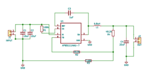
DC-DC power supply circuit diagram.
Technical information
Switching Mode Buck IC
The AP65111A is an adjustable buck converter that provides 5Vs of regulated power at the output. The input voltage range of the IC is 4.5 to 18V. Its output has a direct current of 1.5A.
Characteristics
1. Overvoltage protection. When the FB pin exceeds 115% of the nominal voltage of 0.8V, the regulator will stop switching and the voltage will drop by discharging through the capacitor.
2. Overcurrent protection. When the inductor's peak current exceeds its current limit, it triggers current protection. When the FB pin voltage drops below 0.4V, the device goes into hiccup mode and periodically resets the parts. This will reduce the thermal stress of the IC.
3. Automated no-load/light-load. In case of light load or no load, the IC goes into low load and high efficiency mode. Once it detects a high load, it will automatically enter a pulse width modulation mode for high efficiency.
4. Thermal protection. When the IC junction temperature exceeds 160°C, the IC will shut down. After cooling to 120°C, the IC allows a smooth start.
5. Soft start. The IC has an internal soft start period of 1ms.

AP65111A Pin Diagram
Main Pin Description
PT – a digital pin that turns the IC on and off. Drive EN high to ON and low to OFF. For an automatic start, pull it with 100k resistors.
Facebook – detects the output voltage and regulates it. Connect it to a resistive divider network to set the output voltage.
The circuit design
The circuit design includes the energy storage element. An inductor stores energy in the form of a magnetic field. The inductor in this design acts as an energy storage element.
The equation to calculate the inductor value for the Buck converter:
L = Vout(Vin-Vout)/(Vin.dIL.Fsw)
dIL = Inductor ripple current
Fsw = Regulator switching frequency
The inductor ripple current should be 30 to 40% of the maximum load current. The inductor peak current will be:
IL = Iload + dIL/2
The peak current “decides” the saturation current rating of the inductor. Inductor saturation will decrease converter efficiency. For this application it is possible to choose an inductor between 1 and 10uH.
So, let's use a 6.5uH inductor and calculate the maximum rated current of the inductor:
L = Vout(Vin-Vout)/(Vin.dIL.Fsw)
Fsw = 500kHz
6.5u = 5(12-5)/(12*dIL*500k)
dIL = 0.89A
IL = Iload + dIL/2
Iload = 1.5A
IL = 1.95A
We can then analyze the calculation above. Consider the minimum inductor current to be 25 to 30% above the maximum load current. We must also consider the DC resistance of the inductor to be less than 20m ohms to ensure high efficiency.
The filter element
Input: The input capacitor helps reduce the surge current during the ON state of the device. The rated RMS current of the input capacitor must be greater than half the maximum load current. The ESR of the capacitor must be low due to the high current rate variation (dI/dt) through the input capacitor. For this project, a 22uF capacitor works well.
Output: The output capacitor reduces output voltage spikes, maintains circuit stability, and reduces excess output voltage. It helps in fast transient response and provides current for a few cycles during load transients. An output capacitor with a high value and low ESR is ideal. In this application, we can use a 22uF ceramic capacitor for output.
We can calculate the value of the capacitor with this equation:
Co = L(Io + dIL/2)2/(dV + Vo)2 – Vo2
Feedback Network
Now for the output voltage setting. According to the wiring diagram, resistors R4 and R3 decide the output voltage.
Here is the equation:
Output voltage, Vout = 0.8(1+R4/R3)
R4 = 40.2K, R3 = 7.68K
Vout = 5V approx.
Resistance R2 is also recommended to improve system stability, especially for Vout < 3.3V.
Thermal management
To find out the maximum power that the IC regulator can dissipate, use this equation:
Pd(max) = (TJ – TA)/QJA
Where,
P JÁ and T J. are indicated in the IC data sheets
T J. = maximum junction temperature = 160°
P ALREADY = thermal resistance (attached to the environment) = 120° C/W
T A , = ambient temperature = 30° (according to environmental conditions)
P d(max.) = maximum power dissipation of the device
Putting all the values in the equation above, we obtain:
P d(max) = 1.08 W
This is the maximum power the IC can dissipate without a heatsink – but only under natural airflow conditions.
As power dissipation increases, it becomes necessary to mount a heat sink or fan to dissipate excess heat, otherwise the regulator will malfunction.
Practical observation
V in Input voltage = 12V

**For a current of 1.26A the power dissipation is 1.41W. Since this exceeds the maximum power dissipation limit of the IC, we will need to mount a heatsink to dissipate the extra heat.
Note: To learn more about selecting a heatsink, see this article.
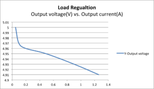
The load regulation curve between output voltage compared to output current.
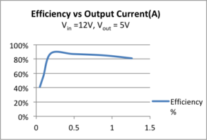
The results observed.

The characteristics of the data sheet.
IC performance
5. Under light load (<100mA), the efficiency is low and below 50%
6. At higher loads, the IC performs as expected, with an average efficiency of 85%
7. Load regulation: Regulated 5V for current <50mA
Precautions
- A capacitor must be connected between the IN pin and ground to regulate the DC input voltage.
- The circuit capacitor must have a higher rated voltage than the input supply voltage. Otherwise, the capacitor will start to leak current due to excess voltage on its plates and will explode.
- Make sure the capacitor is fully discharged before working on a DC power supply.
- The rated current of the inductor must be 1.15 times greater than the output current.
- Never supply an input voltage higher than the operating input voltage range of the IC.
- Avoid shorting the output terminals – this will reverse the current flow in the IC, leading to failures.
- Also, do not short the input terminals – this will generate a large current in the circuit and the circuit components will fail.
- Consider the frequency effect.
PCB Design Guidelines
- Keep power strokes thick and short
- Place the input and output capacitor as close as the IC's input and output pins
- Minimize inductor path length
- Keep voltage and switching nodes away from each other
- Keep all components as close as the IC and try to reduce the PCB size
- Remember: the higher the IC frequency, the greater the switching losses, which reduces efficiency. But a high switching frequency reduces the size of the energy storage element and improves the transient response.
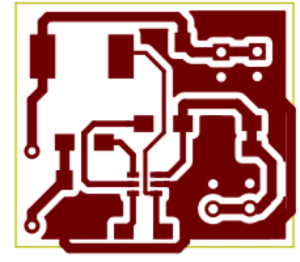
The PCB design layout.
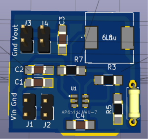
An animated 3D PCB visualization.
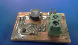
The image in real time.

