ADC is an electronic device that converts analog signals into digital numbers proportional to the magnitude of the voltage. ADC chips like ADC0804, ADC0809 etc. provide 8-bit digital output. The controller device needs eight pins to receive the 8-bit data (for more details about the ADC, see Using the AVR's Built-in ADC). Some applications need higher resolution ADCs (10-bit or greater digital data output) for data accuracy.
The use of parallel ADCs is an option for such applications. However, using parallel ADC will increase the hardware size as a 10-bit parallel ADC will have 10 output lines. Additionally, you may need to use a controller with a higher number of pins. The other option is to use a serial ADC, which requires fewer pins. Since data is transmitted serially, the data transfer rate of serial ADC is low compared to parallel ADC. They can serve as a very good alternative in applications where data transfer speed is not a critical point. This article explores the interface of the ADC0831 serial with ATmega16.
The ADC0831 is an 8-pin single-channel serial ADC that provides 8-bit data output. The input can be single-ended or differential type. Using the differential input option, A/D conversion can be performed for two different voltage levels. The function of each pin is described in the following table:

Fig. 2: Pin name and functions of serialADC0831
1. (Chip selection) – To start the conversion, a value from high to low is provided .
2. V in (+) (Positive Analog Input ) – Positive voltage is applied to this pin. The input range for this is 0 to 5votls.
3. V in (-) (Negative analog input) – Negative voltage is applied to this pin.
4. GND (Ground) – This pin is connected to the circuit ground.
5. V reference (Reference voltage) – This pin is used to define the input voltage range of the ADC.
6. CLK (clock) – The clock pulse is supplied at the CLK pin for synchronization.
7. DO (data output) – This pin is an output pin of ADC, serial output data is available on this pin.
8. Vcc (power supply) – This is connected to the +5 volt power supply.
How serial ADC works:

Fig. 3: Block diagram of serial ADC working with AVR
The above diagram shows a system in which the ADC device receives analog data from the transducer. The controller is used to control the ADC IC and process the converted digital data. The analog signal is given at the V pin at (+). In differential mode, voltage at pin V in (+) must be greater than V in (-) otherwise the output data will not be generated by the ADC. Data conversion is initiated by giving a high to low pulse on the CS pin. In the first clock cycle, the ADC sends the '0' bit to the controller which shows that the following bits are the data bits. The MSB of the converted data is sent first. The timing diagram of the ADC0831 is shown below.

Fig. 4: ADC0831 timing diagram for serial communication on the AVR
Purpose: Convert the analog output voltage of the variable resistor into digital signals using ADC0831 and display it on the LCD.
Circuit Description:
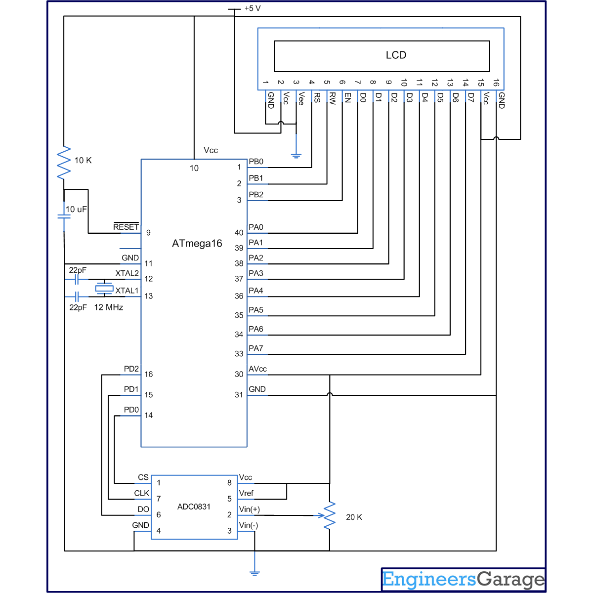
Connection of ADC0831 with ATmega16 is shown in the circuit diagram. The variable resistor output is connected to V in (+) and V in (-) pin is grounded. The CS, CLK and DO pins of the ADC are connected to the microcontroller.
Programming steps:
1. Send a high-low pulse to the CS pin to initialize the conversion.
2. Monitor the status of the D0 bit until it goes low.
3. Send a clock pulse.
4. Receive data bits from DO pin of ADC 0831.
5. Store the data bits into a variable using bitwise operation.
Project source code
 ###

 // Program for ADC 0831 serial interface with AVR microcontroller (ATMEGA 16)
###
Circuit diagrams
| Circuit diagram of how to interface serial-ADC0831 with AVR-ATmega16 microcontroller |  |
Project Components
- ATmega16
- LCD

