A suitably doped crystal diode with a penetrating breakdown voltage is called a Zener diode. From its humble beginnings as a simple semiconductor device to its extraordinary rise to become a luminary in electrical engineering, the Zener diode has fascinated engineers and scientists with its unparalleled capabilities. This remarkable electronic device, named after physicist Clarence Zener, opened up a world of possibilities, pushing conventional limits and pushing the boundaries of traditional diodes. Join us on an enlightening journey as we trace the evolution of the Zener diode, discover its fascinating principles, and discover the specialized applications that have made it an indispensable tool in countless technological advances. Prepare for a breathtaking odyssey through the fascinating realm of the Zener diode, where brilliance meets innovation and possibilities are limitless.
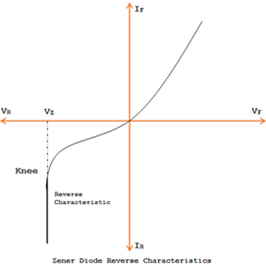
When the reverse voltage of a PN junction crystal diode is increased, a critical voltage, the so-called breakdown voltage, is reached, at which the reverse current increases sharply to a high value. The rupture area is the breaking point of the blocking characteristic curve, as shown in the figure.
American scientist C. Zener was the first to provide an adequate explanation for this groundbreaking transition. Therefore, the breakdown voltage is sometimes called the Zener voltage and the sudden increase in current is sometimes called the Zener current.
The breakdown voltage or Zener voltage depends on the amount of doping. If the diode is heavily doped, the depletion layer will be thin and junction breakdown will occur at a lower reverse voltage. On the other hand, a lightly doped diode has a higher breakdown voltage. When a normal PN junction diode is suitably doped to have a sharp breakdown voltage, it is called a Zener diode.
VI Characteristics of a PN Junction Diode
The VI properties of a PN junction diode reveal a fascinating interplay between voltage and current, revealing the fundamental behavior of this essential electronic component. When we delve deeper into PN junction diodes, we come across a fascinating relationship between the applied voltage and the resulting current flow. First, there is a gradual increase in the forward bias region as the voltage across the diode increases. The diode conducts and allows the flow of electrons, facilitating the passage of current with relatively low resistance. However, a fascinating phenomenon unfolds in the reverse bias region. Here, increasing the reverse voltage causes a negligible current to flow through the diode, creating a high-resistance barrier. It is in this range that the diode demonstrates its unique property: the ability to withstand and block reverse current flow, thus protecting electronic circuits. The VI characteristics of a PN junction diode not only clarify the behavior of this fundamental component, but also provide engineers and enthusiasts with valuable information about its versatile applications in rectification, signal modulation, and more.
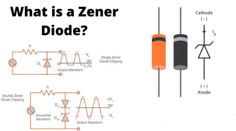
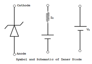
Zener diode symbol and diagram
The circuit symbol of a Zener diode and its equivalent circuit are shown in figure (a). The complete equivalent circuit is shown in figure (b) and the approximate one in figure (c), which looks like a V. battery for example Volt.
The circuit symbol of a Zener diode is similar to that of a normal diode, except that with a little mental effort the line representing the cathode is bent at both ends; You can think of the cathode symbol as the letter Z for “more Zen.”
Zener voltage
Zener diodes are available with Zener voltages from 2.4 V to 200 V. This voltage is temperature dependent. The VzIz product offers maximum power dissipation values ranging from 150 mW to 50 W.
Note the following information about the Zener diode:
-
A Zener diode is similar to a regular diode, except that it is properly doped to ensure a sharp breakdown voltage.
-
A Zener diode is always connected in reverse, i.e. H. biased in the reverse direction.
-
A Zener diode has a sharp breakdown voltage, called Zener voltage V. for example .
-
In direct voltage the properties are exactly those of a normal diode.
-
The Zener diode does not burn out immediately because it has already entered the breakdown region.
Equivalent Circuit Diagram of a Zener Diode
Circuits utilizing Zener diodes can be easily analyzed by replacing the Zener diodes with the corresponding circuit.
A condition
When the reverse voltage across a Zener diode is equal to or greater than the breakdown voltage V, the current increases sharply; in this area the curve is almost vertical. This means that the voltage across the Zener diode is constant in V. for example despite recent changes.
Therefore, in the breakdown region, an ideal can be represented by a battery with voltage V. z, as shown in Fig. Under such conditions, the Zener diode is on.
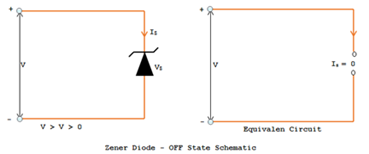
OFF state
If the reverse voltage across the Zener diode is less than V for example but greater than 0V, the Zener diode is in the OFF state. Under such conditions, an open circuit may represent the Zener diode, as shown in Fig.
Classification of insulation materials
Insulating materials are crucial in many industries as they provide electrical and thermal insulation as well as mechanical protection. Understanding the classification of insulation materials is critical to selecting the appropriate material for specific applications. Insulating materials can be broadly divided into organic and inorganic categories. Organic insulating materials include rubber, plastics, resins and synthetic polymers. These materials offer flexibility, excellent electrical insulation properties, and resistance to moisture and chemicals.
Use of Zener diodes
-
As a voltage regulator
-
As a fixed reference voltage in a network for polarization and comparison purposes and for calibrating voltmeters.
-
Like a spike cutter
-
To protect the measuring device from damage caused by unintentional use of excessive voltage.
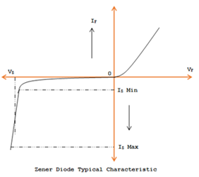
VI Characteristics of Zener Diode
A typical characteristic curve is shown in the negative quadrant of the figure. The forward part is simply that of an ordinary forward biased junction diode.
The important points about reverse properties are
v for example = Zener breakdown voltage
EU zmin = Minimum current to maintain breakage
EU zmax = Maximum Zener current limited by maximum power loss
The inverse function means that V for example remains constant even if I for example increases significantly.
Conclusion
In short, the development of the Zener diode was simply breathtaking. From its discovery by Clarence Zener at the beginning of the 20th century to its widespread use in modern electronics, this semiconductor device has revolutionized voltage regulation and protection systems. Their unique ability to conduct in blocking mode makes them indispensable in various electronic circuits. As technology advances, the versatility and reliability of the Zener diode will continue to be a key element of innovation in the ever-evolving world of electronics.