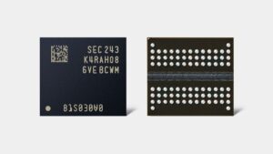
Samsung Electronics announced the development of its 16 gigabit (Gb) DDR5 DRAM built using the industry's first 12 nanometer (nm) class process technology. It also successfully completed product evaluation for AMD compatibility.
 “Our 12nm range DRAM will be a key enabler in driving the adoption of DDR5 DRAM across the market,” said Jooyoung Lee, executive vice president of DRAM product and technology at Samsung Electronics. “With exceptional performance and energy efficiency, we expect our new DRAM to serve as the foundation for more sustainable operations in areas such as next-generation computing, data centers and AI-based systems.”
This technological leap was made possible through the use of a new high-κ material that increases cell capacitance and a proprietary design technology that improves critical circuit characteristics. Combined with advanced multilayer extreme ultraviolet (EUV) lithography, the new DRAM features the highest die density in the industry, enabling a 20% gain in wafer productivity.
“Innovation often requires close collaboration with industry partners to push the boundaries of technology,” said Joe Macri, senior vice president, corporate fellow and CTO of clients, computing and graphics, AMD. “We are excited to collaborate with Samsung once again, especially in launching DDR5 memory products that are optimized and validated on 'Zen' platforms.”
Leveraging the latest DDR5 standard, Samsung's 12nm-class DRAM will help unlock speeds of up to 7.2 gigabits per second (Gbps). This translates into processing two 30 gigabyte (GB) UHD movies in just one second.
The exceptional speed of the new DRAM is accompanied by greater energy efficiency. Consuming up to 23% less power than previous DRAM, 12nm-class DRAM will be an ideal solution for global IT companies seeking greener operations.
With mass production expected to begin in 2023, Samsung plans to expand its DRAM lineup based on this cutting-edge 12nm-class process technology to a wide range of market segments as it continues to work with industry partners. to support the rapid expansion of next generation computing.


