An amplifier is a circuit that can produce an output voltage, which is the product of the input voltage and a value called voltage gain. An operational amplifier ( operational amplifier ) is a kind of amplifier circuit that can perform an operation (addition, subtraction, etc.) on input voltages in addition to simply amplifying the input.
An operational amplifier (operational amplifier) is an electronic circuit made of various active devices (transistors) and passive devices (resistors, capacitors) etc., which is capable of realizing the following common characteristics:
– extremely high voltage gain
-can amplify the input current at the output
-can invert the input voltage at the output
-can produce a sum of input voltages at the output
-can produce a sum of input currents at the output
2) History of the operational amplifier
For every significant invention in history, there must be a time before such an invention when there was a need for such a thing. Before operational amplifiers there were also amplifiers. But they were only designed for constant gain. They were made with vacuum tubes and other components. Furthermore, the maximum gain of a particular amplifier was limited by the specifications of the vacuum tube.
This was really a problem, especially in the early days telephone network. Telephone lines used to be thousands of meters long and amplifiers need to be implemented to amplify the signal. Amplifiers at that time had less gain and were very sensitive to temperature and humidity. At each point in the network, amplifiers with different gains were designed and implemented separately.
Telephone engineers at Bell Labs were trying to figure out a solution to this. Finally, an engineer named Harry Black had an idea. Design a general amplifier circuit with gain many times greater than any normal requirement, and then reduce the gain to the required levels using a negative feedback system with that amplifier. Bell Laboratories successfully designed this circuit using vacuum tubes before 1940. This ingenious idea triggered the era of operational amplifiers.
The term operational amplifier first appeared in a patent produced by Karl D. Swartzel of Bell Labs in 1941. This amplifier was capable of performing a summing operation on input voltages.

First operational amplifier circuit
(header = History of Op Amplifier Contd…)
The above circuit was able to add the input voltages marked as A, B and C. Negative feedback was applied through a variable resistor marked as 16 in the circuit. This op amp circuit had only one input terminal which inverts the input. We will discuss about inverting input and non-inverting input later in this article.
In 1947, Loebe Julie developed an operational amplifier with two input terminals (inverting and non-inverting), as we see in current operational amplifiers. The first commercial operational amplifier was released by GAP/R incorporated based on Loebe Julie's design. The model name was GAP/R K2-W.

First commercial operational amplifier
Early analog computers operated based on the summation of voltages and operational amplifiers were widely used in them for voltage operations. This has made the term operational amplifier very popular in the electronics industry.
After the invention of transistors, they replaced vacuum tubes in every possible circuit. Consequently, in operational amplifiers too, bulky vacuum tubes were replaced by transistors. This was the beginning of the design of operational amplifier circuit modules. They are built on a small-sized circuit board, which can be easily connected to other larger circuit boards. This results in considering the operational amplifier as an electronic component in itself, although it is constructed with the help of other basic components. GAP/R also produced a commercial solid state operational amplifier, the model name was GAP/R P45.

First commercial solid-state operational amplifier
Later it was discovered that several transistors can be integrated on a single silicon chip and thus the size of the entire circuit can be reduced several times. Around the 1960s, transistor-based integrated chips (IC) were developed. Operational amplifiers were the first transistor-based circuits integrated into ICs. It was Fairchild Semiconductor who released the first commercial operational amplifier IC, the ?A702. It was in 1968 that the classic and most successful operational amplifier IC of all time, the ?A741, was released by Fairchild. It was designed by Dave Fullagar. Even today the same design is produced by Fairchild and also by other manufacturers.

uA741
(header= Basic functional blocks of an operational amplifier)
3) Basic functional blocks of an operational amplifier
As we already mentioned, although the operational amplifier is considered an electronic component, it is actually made up of several other basic electronic components such as transistors, resistors, capacitors, etc. Almost all op amp ICs have the same basic functionality internally. blocks, built by basic electronic components. These functional blocks are, namely,
– Differential input amplifier
– Voltage amplifier
– Output power amplifier
3.1) Differential input amplifier
A differential amplifier is the most important module within an operational amplifier. Input voltages are applied to the pins of the differential amplifier block. Let us discuss the differential amplifier in detail.
A normal amplifier amplifies the entire signal voltage with respect to ground and is fed to the output. And these amplifiers typically have a single input and obviously a single output. For example, if we give 5V as ground-referenced input to a normal amplifier and the voltage gain of the amplifier is, say, 2, then the output will be 10V, provided the circuit receives a supply voltage greater than 10V.

Voltage Amplifier
In the circuit shown above, you can see an amplifier that is connected to a 20V power supply and has a voltage gain of 2. When a voltage of 5V is fed to the single input pin, the output will be 10V. GND is considered a common reference point for both input voltage and output voltage.
The differential amplifier, on the other hand, only amplifies the difference between the two input voltages. For example, if the gain of the differential amplifier is, say, 2, and if we give a voltage of 3V to one of its input pins and on the other pin we give a voltage, say 5V. Now the difference between these two voltages, i.e. (3~5=2) is amplified and will be available at the output. Therefore, the output voltage is 2V*2=4V.
Therefore, a typical differential amplifier rejects or masks the effect of common mode voltage on its output. Common mode voltage means the voltage that is common to both input pins. For example, if we apply a voltage of 5V to one input and 3V to another input pin, the common mode voltage will be 3V.
Therefore, if the input voltages are,
Input voltage1, V1 = 5V,
Input voltage2, V2 = 3V, so
Common mode voltage = 3V, and
Differential voltage = 5 ~ 3 = 2V

Differential voltage
The differential amplifier simply rejects the common mode voltage and amplifies only the differential voltage.

Differential amplifier
Differential amplifiers basically have two power supplies, two inputs and two outputs. The two outputs are then combined into a single output using a circuit called current mirrors. The voltages on the input pins are called differential input voltage and the voltages on the two output pins are called differential outputs.

Transistor-Based Differential Amplifier
(header= Differential Input Amplifier Cont.…)
In the above circuit, there are two input terminals, marked as Vin+ and Vin-. The output voltage is obtained differentially across the collectors of two transistors.
The two output pins can be combined into a single output pin using a differential for single-ended conversion. We call this current mirror conversion circuit.

Current mirror in the differential amplifier
The inverting input produces a negative amplified voltage at its output and the non-inverting input produces a positive amplified voltage at its output. The differential to single terminal converter converts this differential voltage into single terminal voltage.

Single-ended conversion
Let's look at the example in Figure: 7. Suppose 5V is applied to the non-inverting pin and 3V is applied to the inverting pin of the differential amplifier. The gain of the amplifier is 2 and therefore the non-inverting pin results in an output voltage of 2*5=10V and the inverting pin results in a voltage of -2*3=-6V. After single-ended conversion, the output voltage will be 10-6, that is, 4V.

Single-ended conversion example
As shown in Figure: 6 and Figure: 7, one of the main advantages of differential amplifier among normal amplifier types is common mode voltage rejection. Suppose we have a two-line input and we are applying the two input lines to the input pins of a differential amplifier. Suppose somehow noise gets into the input lines and affects both lines equally. Since the noise is common to both inputs, it will be rejected at the amplified output. Consequently, we obtain an amplified signal without noise at the output.
Since the differential amplifier only produces the signal voltage at the output, we can avoid the bulky coupling capacitor at the output end.
Differential amplifier is normally realized using BJT or MOSFET with two identical devices and we call them differential pair
3.2) Voltage Amplifier
An amplifier is a device that can simply produce an output voltage or current, which is the product of the input voltage or current by a value called gain. Therefore, a voltage amplifier is an amplifier that can produce a voltage gain at the output. Gain is the ratio between the output voltage and a given input voltage and is expressed in decibels (dB).
gain = output voltage/input voltage
gain = 10log (output voltage/input voltage) dB
In an operational amplifier, the output of the differential amplifier is amplified using a very high gain amplifier, generally Class A type amplifiers are used.
(header = output power amplifier)
3.3) Output power amplifier
The output of the voltage amplifier may have amplified voltages, but its current intensity is much lower. These signals will be easily loaded into the output. Therefore, it is necessary to amplify its power by amplifying the current, maintaining the same voltage at the output. This type of amplifier is called current amplifier, buffer amplifier, emitter follower, etc. In 741 classAB, push-pull emitter follower is used.
3.4) Internal architecture of the 741

741 internal diagram
In the above figure, you can see the input pins, non-inverting input and inverting input are part of the input differential amplifier. This section is marked inside the blue rectangle.
The output pin originates from the push-pull power amplifier forms by transistors Q14 and Q20. This section is marked with a cyan rectangle. The voltage amplifier is marked inside the magenta rectangle. The red rectangle that includes transistors Q8 through Q13 highlights the current mirrors.
(header = symbol of operational amplifier and dual power supply)
4) Operational amplifier symbol
The most important functional block of the operational amplifier is a differential amplifier. It is appropriate to say that the operational amplifier is nothing more than a differential amplifier with very high gain. Consequently, the symbol for an operational amplifier is the same symbol we use to represent a differential amplifier. The following symbol is shared by both differential amplifier and operational amplifiers.

Symbol for operational amplifier
5) Dual power supply
In the above figure itself, you can see that two power supplies are used. +Vsupply represents positive voltage and –Vsupply represents negative power supply. It is assumed that these supply voltages have equal magnitude with respect to a common point (ground GND), but with opposite polarity. We call this power supply a dual power supply.
Most op amp ICs require dual power supply for proper functioning.
Therefore, before we start with any op amp circuit, we must develop a dual power supply. Let's see how to design a dual power supply.
Remember that a dual power supply not only has a positive and negative voltage, but it also has a ground terminal. Furthermore, the magnitude of positive and negative stresses relative to the ground must be exactly the same.
We can realize such a circuit using a simple potential divider, as shown below.

Simple double supply
Resistors must be of the same type and same value. The only problem with the above circuit is the charging effect. If either the positive or negative side is heavily charged compared to the other side, the circuit may become unbalanced.
Also, if you are wondering where to get these positive and negative supply voltages, let's look at the circuit below. It has a step-down transformer, rectifier and positive and negative regulator ICs.
The circuit for a dual regulated power supply is shown in the following figure
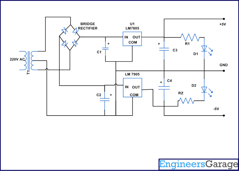
Regulated Dual Supply
Component specifications:
T1=Step-down transformer, 7.5-0-7.5, 1A
C1=C2=C3=C4=100uf, 25V electrolytic
R1=R2=1KE, 1/4W
U1=LM7805
U2=LM7905
D1=LED (red), 3mm
D2=LED (green), 3mm
(header = component significance)
Component Significance:
T1: If you use a transformer with an output voltage greater than 7.5V, such as 9V, 12V, etc., you will get more voltage regulation. The IC 7805 can be safely used in transformers up to 14V. If you use a transformer with a current rating greater than 1A, such as 2A, 3A, etc., you can conduct more load.
C1 to C5: Output regulation can be improved by further increasing the value of these capacitors. Extreme stability can be achieved using 1000mfd capacitors.
R1, R2: The brightness of the indicator LEDs can be increased by decreasing the value of these resistors. LEDs can be used safely with resistor values above 220 ohms on 5V supply.
U1, U2: If we need any other voltage at the output, just change these ICs. Regulated ICs are commonly available up to 12V, 7812 and 7912.
For this entire article, +5V is VCC and -5V is VEE
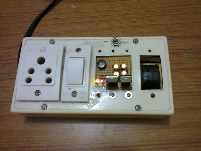
Dual power supply image
The image above is actually the dual power supply built by me. The circuit is exactly the same. It turns out that I built the circuit inside a distribution box, with a switch and socket, so that it would be safe and easy to handle.
Beginners should note that simply connecting the circuit according to the circuit diagram and making it work is one thing and building the circuit in the form of a product is something else entirely. In this tutorial I will only show the basic operating circuit and the image or video of the finished prototype and the rest is up to the reader.
The following image shows how I connect my power supply to the breadboard using jumper wires.
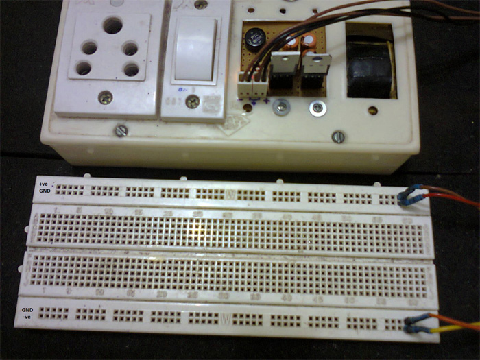
Connecting a dual supply to the breadboard
(header = 741 Op Amplifier Features)
6) 741 Op Amplifier Features
The 741 is a versatile op amp IC and is the best op amp IC for beginners. The design was first released by Fairchild and is still in production. Nowadays, other manufacturers also produce operational amplifier IC with the same name and design.
The commonly available 741 is an eight-pin in-line dual-package operational amplifier IC. It only has a single op amp module inside it and requires dual power supply.

Image of the 741 operational amplifier
6.1) Pinouts
The pinout of the 741 op amp is shown below. Pins 2 and 3 are input pins and pin 6 is the output pin. Pins 4 and 7 are provided for dual power supply.

Pinout of 741
An operational amplifier is assumed to have zero output voltage whenever the input differential voltage is zero. But in practice this is difficult to achieve, due to certain current incompatibilities at the input terminals. The 741 has two terminals to set the output voltage to zero when the input voltage is zero. The pins provided for this function are called offset null.
In this article we are not interested in using these offset null pins. Modern operational amplifiers have an internal mechanism for adjusting the offset voltage.
Among the input pins, pin2 is called inverting input and pin3 is called non-inverting input. These terms are very important in relation to an operational amplifier and we will discuss them in detail in the following sections.
(header = Testing an IC 741)
6.2) Testing an IC 741
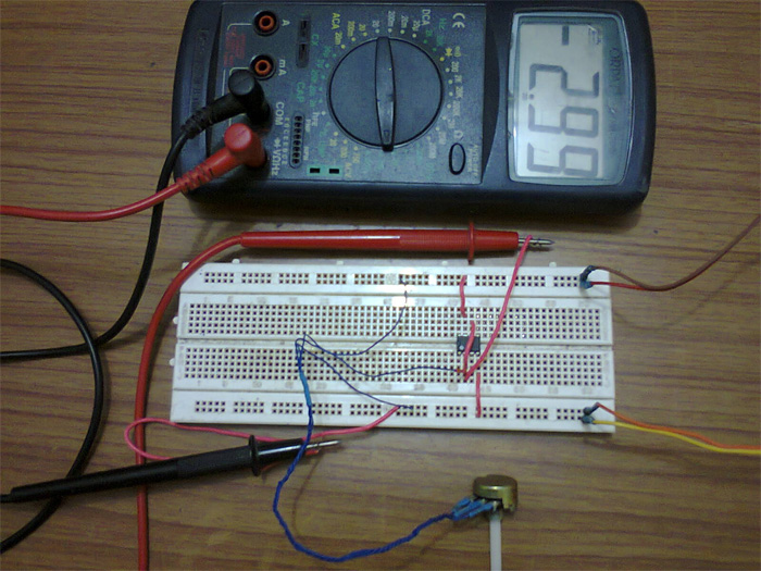
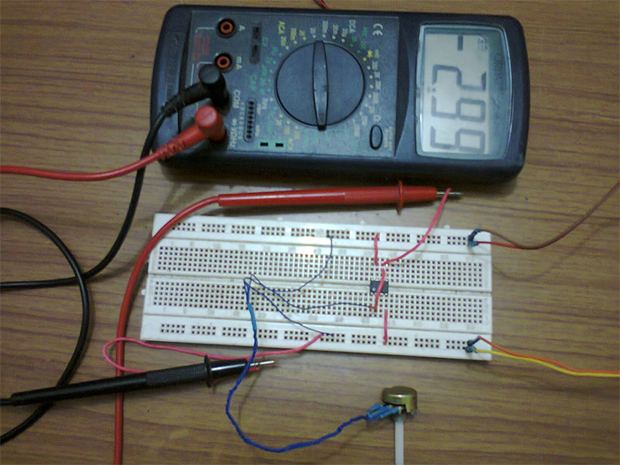
It is important to make sure that the operational amplifier we have is working correctly before we proceed with new experiments. Here is a simple method to test an IC 741, with minimal components and circuit connection

Test circuit for LM741 non-inverting pin
Here we have shorted pin 6 and pin 2 of the op amp. This circuit is commonly called a voltage follower. A voltage is applied to pin 3 of the operational amplifier through the variable resistor (10K). All we need to do is check whether the voltages V1 and V2 are exactly the same or not. Check them using a multimeter. If they match exactly, then you have a perfectly working op amp and are now ready for further experiments.
The same check can be done by also applying an input voltage V1 to the inverting pin and checking the output voltage V2 as shown below.

Test circuit for LM741 inverter pin
(header = Testing a 741 IC Contd…)
Images of the test performed are shown in the following figures.


Test circuit image for LM741 non-inverting pin
Test circuit image for LM741 inverter pin
(tagsToTranslate)pic


