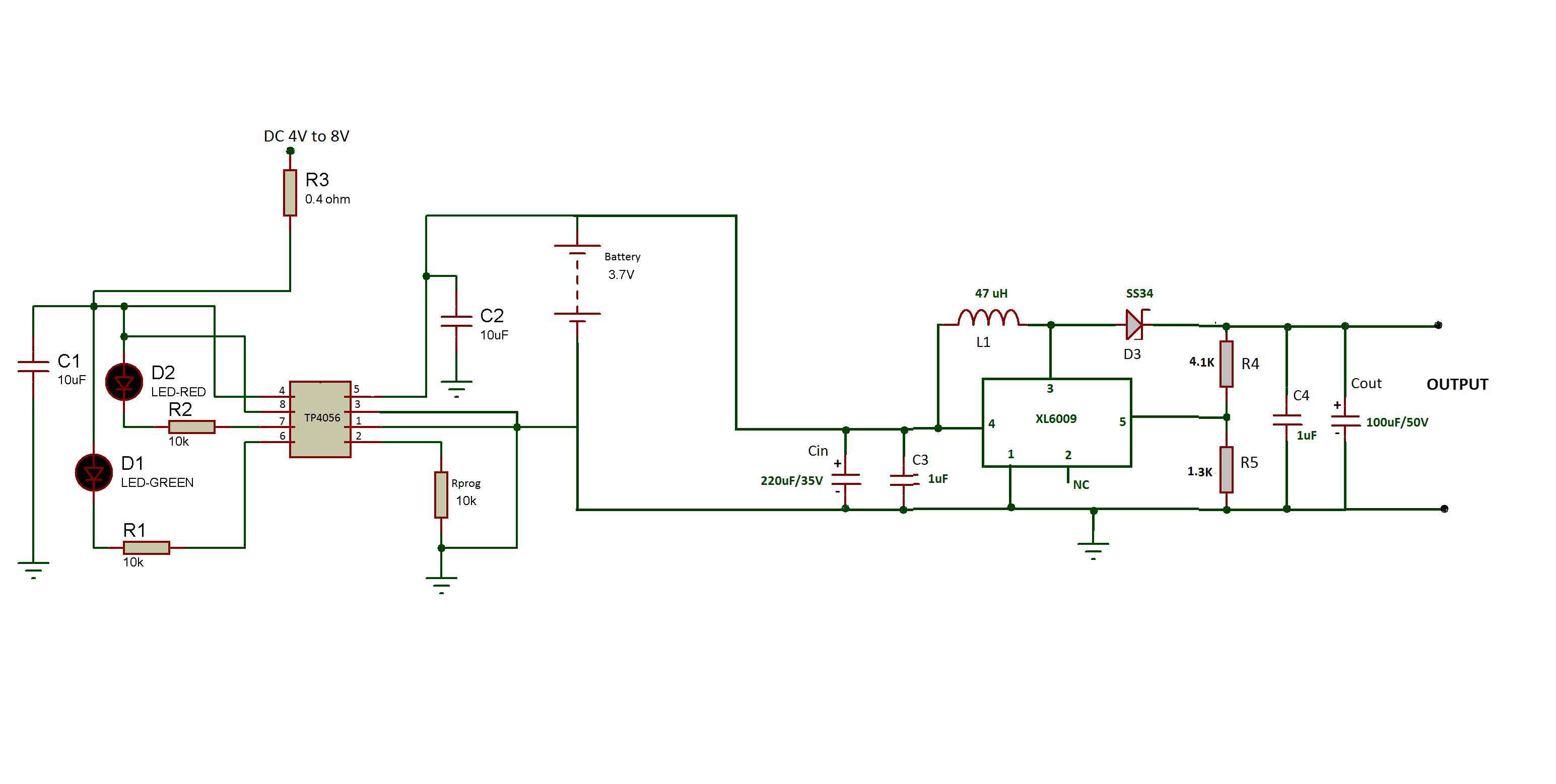
As the popularity and use of smartphones and tablets has grown, the demand for convenient, portable power supplies has also increased. Smartphones and tablets come with a battery that drains after 4 to 5 hours of use. As a solution to this problem, power banks were introduced into the market for frequent users. These power banks also come in handy when the user is on a long trip and does not have the facility to charge their phone or tablet. A power bank is basically a portable device that can supply power to devices like smartphones and tablets through the USB port. The power bank itself can be charged via the USB port and stores charge that can later be used to power other devices.
In this experiment, a power bank will be designed that can provide a power output of 5V/4A. The power bank will be built with a 3.7V Li-ion battery and will have a charger circuit built with IC TP056 and power boost circuit at the output. The lithium-ion battery will store the charge and then the charge stored in the battery will be used to power the devices. To store the charge, first the Li-ion battery needs to be charged using a charger circuit for which IC TP056 is used. This IC is commonly used to charge lithium-ion batteries. The IC is specially designed to charge a single 3.7V Li-ion battery and can provide maximum charging current of 1A.
Cell phones and most electronic devices need 5V to power up, but the lithium-ion battery will provide a maximum voltage of 4.2V. Therefore, you will need a power amplifier circuit that can amplify the output power to 5 V. To amplify the energy stored in the battery, the XL6009 regulator IC is used, which will increase the DC power of the battery to a regulated 5 V DC. The XL6009 provides a maximum current of 4 A at the output (according to the data sheet). Therefore, the power bank designed in this electronics project will provide an output power of 5V/4A.
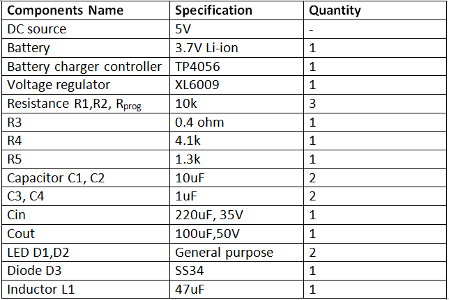
Required components
Fig. 1: List of components required for Power Bank
How the circuit works –

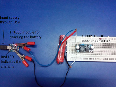
Fig. 2: Power Bank prototype designed on a breadboard
The power bank circuit has two building blocks – 1) Battery recharging circuit and 2) Output amplifier circuit. If the required output voltage were only 3.7V or 4V, the amplifier circuit would not be necessary. However, the required output voltage is 5V, so the amplifier circuit at the output of the device is mandatory. According to the circuit sections, the device also operates in two stages – 1) Charging the battery and 2) Capturing the battery output through the amplifier circuit.
1) Li-ion battery charging with TP4056 charger
In this electronic project, a 3.7V lithium-ion battery is used to store the charge which is fully charged when the terminal voltage reaches 4.2V. As any battery is charged, the voltage output at its terminals continues to increase. Each battery has a peak terminal voltage value at which the battery is fully charged. Thus, the battery charge percentage is also estimated by measuring the terminal voltage. The lithium-ion battery needs to be handled carefully as it may catch fire due to overcharging. Therefore, to charge the lithium-ion battery, special ICs like TP4056 IC are used, which automatically disconnects the battery from the input source when the battery is fully charged.
TP4056 is an IC specially designed for charging 3.7V Li-ion batteries. This is a linear battery charger controller with constant current and constant voltage. By adding a single programmable resistor, the IC can be used to charge a 3.7V lithium-ion battery. The charging voltage is fixed at 4.2V and the charging current can be set by adding some resistor and capacitor depending on the battery to be charged. The IC also provides internal thermal protection and current limiting. There is no need to add extra blocking diode due to the internal P-MOSFET that blocks reverse current.
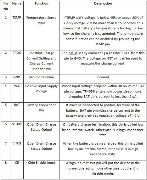
IC TP4056 comes in SOP package, which makes it ideal for use in portable devices. It also requires fewer external components, no less than a few resistors and capacitors. The IC has 8 pins with the following pin configuration –
Fig. 3: Table listing the pin configuration of the IC TP4056
The IC requires a minimum voltage of 4V to 8V for its operation. It can provide a maximum charging current of 1000mA to the battery and a fixed 4.2V at the output. The circuit given in the IC datasheet is used to design the charger.
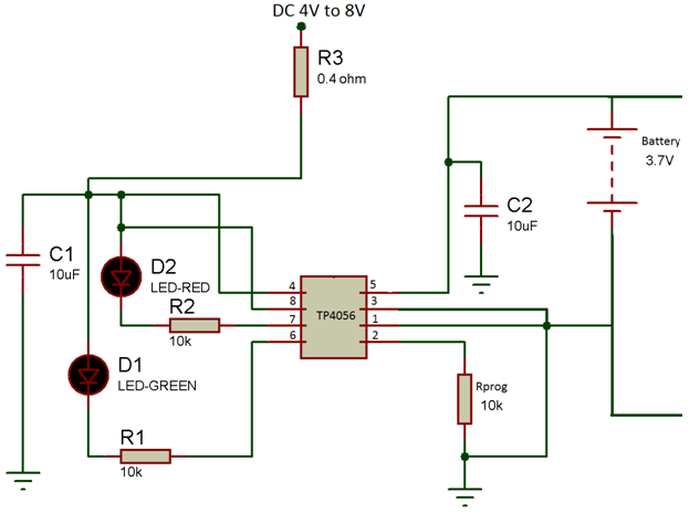
Fig. 4: Circuit diagram of Power Bank battery charger based on IC TP4056
To decide the value of the battery charge current , the resistor must be connected to the PROG pin as described in the data sheet.
For load current of 1000mA R program can be calculated as follows –
EU stick = ( V PROG. /R PROG. )*1200 (V PROG. = 1V)
R program = (V program /I stick )*1200
R program = (1/1)*1200
R program = 1.2k
The battery must be connected according to the polarity indicated on the IC, as the IC TP4056 does not have any protection circuit against polarity reversal.
y Battery charge indicators
For visual indication of charging completion and battery charge status, LEDs can be connected to pins 6 and 7 of the IC. When input power is supplied to the circuit, the red LED on pin 7 lights up, indicating the charging status of the battery. When the battery voltage reaches 4.2V, the battery will draw less current. When the charging current drops to 1/10th of the programmed current (1000mA), charging will end. The green LED on pin 6 will illuminate and give a visual indication that the battery is fully charged (as the terminal voltage has reached 4.2V).
2) Extracting the output from the battery through the voltage amplifier and regulator circuit –
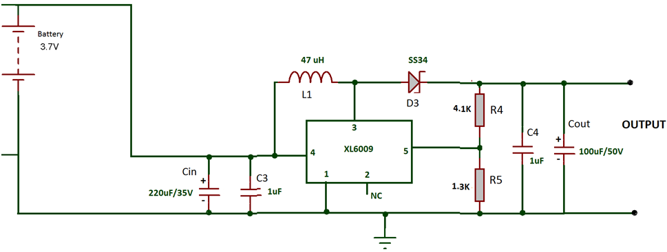
Once the battery is fully charged by the TP4056 charger circuit, it is ready to provide output. The output voltage of the lithium-ion battery needs a boost converter that will increase the battery's output voltage to 5V.
A boost converter is used to convert the input DC signal to the higher voltage level. The XL6009 regulator IC is used for boost converter circuit that provides regulated and amplified voltage. This boost converter amplifies the signal to about 1.6 times the battery input signal with an efficiency of 94%. The XL6009 is a DC to DC converter capable of generating positive or negative output voltages with the input voltage in the range of 5V to 32V.
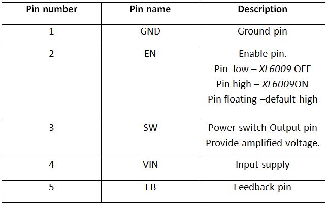
The IC has integrated N-channel power MOSFET and fixed frequency oscillator that allows it to provide stable output over a wide range of input voltages. The IC is specially designed for use in automotive boost, inverter converters, notebook adapters and portable electronic equipment. The IC has features like frequency compensation, thermal shutdown, current limiting and soft start. It is available in package T0263-5L. The XL6009 will operate with an input supply voltage of -0.3V to 36V and can provide an output in the range of -0.3V to 60V. The IC has five pins with the following pin configuration –
Fig. 5: Table listing the pin configuration of the XL6009 regulator IC
The circuit specified in the IC datasheet for typical boost converter application is used in this project.
Note : You can find the XL6009 boost converter circuit in the “Circuit Diagram 2” tab.
At the input and output of the regulator, capacitors (Cin and Cout) are used, which reduces unwanted ripples and noise in the signal. Cout provides a smooth, regulated DC voltage at the output. A small value 1uF capacitor (C4) is also connected in parallel with the high value capacitor Cout to reduce the ESR (equivalent series resistance) at the output (as high value capacitors have high ESR).
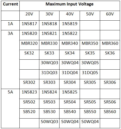
The inductor connected between pins 3 and 4 plays an important role in the boost converter. The main function of the inductor is to store current. The higher the value of the inductor, the greater the current stored in it, but a high value inductor will also have a larger size. Therefore, an inductor must be selected that can supply the desired current at the output. In the project, a 47 uH inductor (L1) and a Schottky diode (D3) are used. The SS34 diode is chosen because it has a lower voltage drop and works well at high frequency. A list of Schottky diodes suitable for the IC according to the current demand and input voltage can be found in the IC XL6009 datasheet. For convenience, the table is precisely repeated below –
Fig. 6: Table listing Schottky diodes suitable for XL6009 regulator IC
Fig. 7: Circuit diagram of the inductor and Schottky diode connected to the XL6009
Internally, the XL6009 has an N-channel power MOSFET with a fixed oscillator frequency (as shown in figure 4 below). This MOSFET acts as a switching transistor and oscillator that generates a square wave of around 400kHz (according to datasheet). During the positive half cycle of the square wave, the inductor stores some energy and generates a magnetic field so that the left terminal of the inductor has a positive voltage and the right terminal is negative. Therefore, the anode of the diode is at lower potential and acts as an open circuit.
The base of the MOSFET receives positive voltage and the MOSFET is turned ON. Thus, all current from the supply flows through the inductor to the MOSFET and finally to ground.
Fig. 8: Circuit diagram showing the negative charge cycle of the XL6009 internal MOSFET
During the negative half cycle, the MOSFET is turned off. Due to this, the inductor cannot charge. Now, the current in the inductor generates a reverse emf (according to Lenz's law) which reverses the polarity of the inductor (as shown in the image below). Therefore, the diode is forward biased. Now the charge stored in the inductor starts discharging through the diode and a regulated voltage is obtained at the output.
In this case, the output voltage now depends on the charge stored in the inductor; the greater the charge stored, the higher the output voltage. Therefore, if the inductor charging time is longer, the charge stored in the inductor also increases. Thus, they become two voltage sources as input, one is an inductor and the other is the input power. Therefore, there is always an output voltage greater than the input voltage.
Fig. 9: Circuit diagram showing the positive charge cycle of the XL6009 internal MOSFET
Resistive voltage divider circuit:
To set 5V at the output of the XL6009, an external resistive voltage divider circuit is used on the feedback pin (pin 5) of the regulator IC (as in the image below). This feedback pin senses the output voltage and regulates it.
Fig. 10: Circuit diagram of the voltage divider connected to the XL6009 output pin
ó Calculating the output voltage
As the internal feedback threshold voltage of XL6009 is 1.25V. This means there is a constant voltage on pin 5 and a constant current will flow through R4 as well as R5. Therefore, the sum of resistor drop across R4 and R5 gives V out as
V out = 1.25*(1+(R4/R5))
As R4 = 4.1k and R5 = 1.3k
V out = 1.25*(1+(R4/R5))
Putting the values R4 and R5 into the equation above
Theoretical observation, V out = 5.2 V (approx.)
The output voltage is not exactly 5V because any device that requires 5V does not work exactly on 5V. It needs a voltage higher than 5V due to some resistive losses and drops in the device. To increase the input signal to 5V, any boost converter modules available on the market can also be used. XL6009 booster boards are also available that provide a constant, regulated voltage of 5V at the output.
Test -
After connecting all the components, 5V is supplied to IC TP4056 which starts charging the lithium-ion battery. The battery output voltage acts as an input to the boost circuit. Therefore, the input voltage to the lithium-ion battery boost/voltage circuit, V in = 4.2 V when the battery is fully charged. The boost circuit amplifies the input and provides an output voltage of 5.18 V. Now, when connecting different loads to the output, different values of load current are observed, which are as follows –
Fig. 11: Table listing power bank output current for different loads
The power bank designed in this project can be used to charge any electronic device that requires a maximum regulated current of 5V and 4A for its operation. The power bank designed in this project has an efficiency of around 94% and due to the use of suitable ICs it has internal overvoltage and thermal protection. The power bank is automatically cut off from the source when fully charged and has LED indicators for charge and full charge indications. Care must be taken that the battery is not discharged by connecting a load during the battery charging process. Charging and discharging simultaneously may reduce battery life and damage the TP4056 IC.
Circuit diagrams
| Circuit-Diagram-Charger-Power-Bank- |
 |
| Circuit Diagram-Power-Bank- |
 |
