PN Intersection
The voltage-ampere characteristic or VI of a PN connection is the curve between the voltage at the connection and the current in the circuit. Typically, voltage is plotted along the X-axis and winding is plotted along the Y-axis.
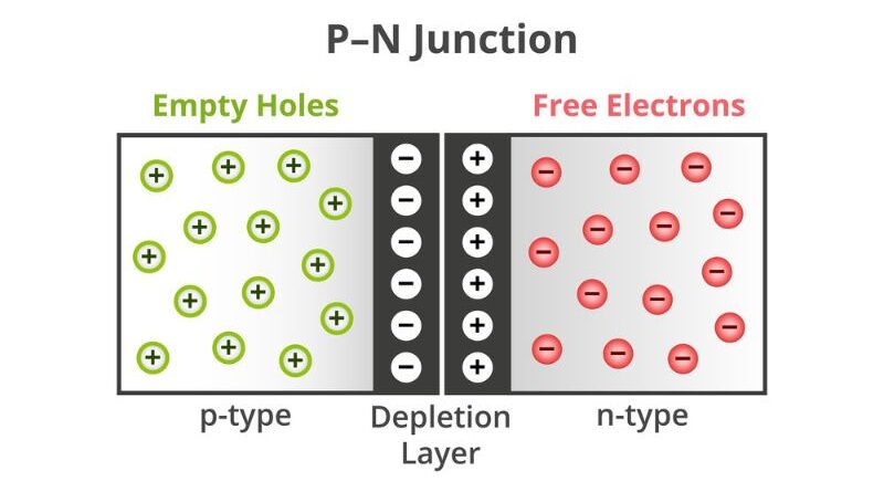
At the center of a PN junction is the connection between a P-type semiconductor region, in which atoms have excess positive charge carriers (holes), and an N-type region, in which particles are doped to have excess carriers. negatively charged (electrons). ) View. This meeting of opposites creates an interface with remarkable properties.
Depletion area
When the P and N regions come together, the so-called depletion zone is created. In this region there is a lack of free charging operators due to the attraction of opposing charges. As a result, an electric field forms across the connection, creating a barrier that resists current flow.
Balance and potential barrier
In the absence of an external bias voltage, the built-in potential barrier prevents any significant movement of the charge carriers. This balance provides the basis for understanding the behavior of PN junctions under different conditions.
Direct bias
By applying a positive voltage to the P-type material and a negative voltage to the N-type material, the potential barrier is reduced. This process is called direct tension. As the boundary becomes smaller, electrons move from the N side to the P side and holes move in the opposite direction. This movement of charge carriers represents a flow of electrical current.
Reverse polarization
On the other hand, applying a positive voltage to the N-type material and a negative voltage to the P-type material increases the potential barrier. This is a reverse voltage. The wall becomes even stronger and makes it difficult for charge carriers to flow through the connection. However, due to the minority carriers, a small reverse current, the so-called leakage current, still remains.
Advancement and Zener effect
At high reverse voltages, a phenomenon called rupture may occur. The Zener effect increases the electric field to such an extent that electron-hole pairs are released through quantum tunneling. This leads to a sharp increase in current, which is often used to regulate voltage. Avalanche breakdown caused by carrier collisions also results in increased current and is useful in applications such as photodiodes.
Applications in practice
Diodes, the simplest PN junction devices, are essential for rectifying AC to DC, protecting circuits against reverse voltage, and more. Bipolar junction transistors (BJTs) and field effect transistors (FETs) use current control between the P and N regions to amplify signals and act as switches in digital logic.
Temperature Effects and Future Trends
Temperature has a significant impact on the behavior of PN junctions, influencing carrier concentrations and the width of the depletion zone. As technology advances, researchers are constantly exploring new materials and structures to improve the performance and efficiency of PN junction-based devices.
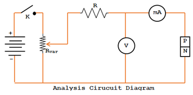
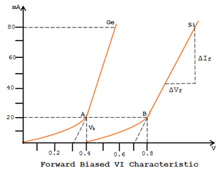
Direct characteristic VI
- A typical VI characteristic for a forward-biased PN junction is shown in the following figure.
- It can be seen that the direct crisis increases exponentially with the applied direct voltage. However, at normal room temperature, a potential difference of about 0.3 V is required before a reasonable amount of direct current begins to flow in a germanium compound.
- This voltage is called threshold voltage V. º (OR) ON VOLTAGE (OR) KNEE VOLTAGE V k . Its value for silicon junctions is about 0.7 volts.
Characteristics of Reverse-Biased VI
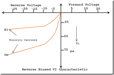
The reverse voltage characteristic VI of a PN junction shows its behavior under the influence of an applied reverse voltage. Let's explore the key points of this fascinating phenomenon in bullet points:
Expansion of the depletion zone
The reverse voltage increases the width of the depletion zone and creates a stronger electric field across the junction. The electric field pushes the majority carriers (electrons in the N-type and holes in the P-type) away from the junction, thus widening the barrier.
leakage current
Despite the widened barrier, a small current, called leakage current or reverse current, flows through the connection. This current is created by minority carriers (minority electrons in P-type and minority holes in N-type) crossing the junction due to heat generation and diffusion.
Current-voltage relationship
The reverse current remains relatively constant in the reverse band and increases as the reverse voltage becomes more negative. The relationship between current and voltage in this range is not linear and the current is typically in the nanoamperes to microamperes range.
Collapse phenomenon
At a critical reverse voltage, the so-called breakdown voltage, an abrupt increase in reverse current occurs. The phenomenon of rupture in the current-voltage relationship is a critical aspect in the study of electrical and electronic systems. When a voltage is applied to a conductor or semiconductor device, the current flowing through it typically increases linearly with the voltage according to Ohm's law.
There are two types of feed mechanisms: Zener feed and avalanche feed.
Zener Advance: Occurs in heavily doped junctions where the electric field is strong enough for electrons to tunnel through the depletion region.
Avalanche Overview: It occurs in lightly doped junctions, where high-energy electrons gain enough kinetic energy to collide with atoms and release more charge carriers.
Influence of temperature
Temperature influences the characteristics of the barrier, affecting the concentration and mobility of carriers.
Higher temperatures can lead to increased return current due to increased carrier generation.
Limitations and considerations
A reverse voltage greater than the breakdown voltage can cause permanent damage to the PN junction.
Extreme reverse voltage can cause thermal runaway and device failure.
Future trends
Researchers continue to explore innovative materials and designs to improve the performance and efficiency of PN junctions under reverse bias conditions.
PN connection with combined forward and reverse bias
- The following figure shows the combined characteristics of forward and reverse VI for Ge and Si.
- The leakage current of the Ge compound is much higher than that of the Si compound.

Direct bias
- Forward bias applies a voltage that lowers the potential barrier across the PN junction.
- Most of the carriers (electrons in N-type and holes in P-type) move across the junction, resulting in current flow.
- In this mode, the PN junction is a conductor that allows the desired current to pass.
Reverse polarization
- The reverse trend creates a wider exhaustion zone, increasing the potential barrier.
- Most carriers are moved away from the connection, minimizing current flow.
- A small reverse leakage current flows due to minority carriers (minority electrons in P-type and minority holes in N-type).
Cropping and saturation
- As the forward voltage increases, the current through the connection increases exponentially. This is the saturation range.
- At a certain point the current reaches a maximum, beyond which it remains constant despite the increase in voltage. This is the shutdown area.
- When transitioning between these two areas, the PN junction changes from highly conductive to weakly conductive.
Combined operation
- When the PN junction changes from forward to reverse bias, the stored charge carriers must leave the intersection.
- This process, called reverse recovery, requires time during which a temporary reverse current flows.
- For high-frequency applications, efficient reverse recovery time management is critical.
Diodes and rectification applications
- The combined operation of forward and reverse bias forms the basis of diode rectification.
- Diodes allow current to flow in one direction and prevent flow in the other, which is essential for converting alternating current to direct current.
Transition effects and switching speed
- Switching between forward and reverse bias causes transient effects due to charge storage in the depletion zone.
- Faster switching speeds are desired in modern electronics, which brings with it the need for optimized diode designs.
Junction Capacitance
- With matched bias, the PN junction acts as a variable capacitor due to the change in width of the depletion region.
- This junction capacitance impacts high frequency applications and must be taken into consideration in circuit design.
Amplification in transistors
- Transistors use a combined bias voltage to control current flow and amplify signals.
- Bipolar junction transistors (BJTs) and field effect transistors (FETs) rely on the behavior of PN junctions to regulate and amplify current.
Influence of temperature
- Temperature influences forward and reverse polarization properties, changing the concentration and mobility of carriers.
- To ensure stable operation of the device under different conditions, this influence must be understood.
Role in modern electronics
- In modern electronics, combined polarization behavior is important in manufacturing a variety of devices, from diodes to complex integrated circuits.
- Engineers use these properties to design efficient and reliable electronic systems.
important terms
Break the tension
It is the minimum reverse voltage at which the PN junction collapses with a sudden increase in reverse current.
Knee tension
Peak reverse voltage
Understanding PN Junctions
PN junctions form the backbone of modern semiconductor devices and play a central role in their operation. A PN junction is formed by connecting a P-type region with an excess of positively charged carriers and an N-type region with many negatively charged faces. This combination results in a depletion region, the space charge region, which acts as a barrier to current flow. Understanding the VI characteristics of PN junctions is fundamental to understanding their behavior and the performance of associated devices, such as diodes and transistors. By studying VI properties, we can gain valuable information about the conduction properties, polarization effects, and applications of PN junctions in electronic circuits.
Conclusion
In summary, studying the VI properties of PN junctions provides a deep understanding of the behavior and functionality of semiconductor devices. Engineers and researchers gain valuable information about the conduction characteristics, bias effects, and active areas of diodes, transistors, and other electronic components by analyzing the relationship between voltage and current across a PN junction. VI properties allow us to determine the forward and reverse bias behavior of PN junctions and explore their applications in various circuit designs. By deepening our understanding of these properties, we can harness the full potential of PN junctions to develop innovative and efficient electronic devices that drive technological progress. Continued research and exploration of VI properties will undoubtedly contribute to the development of cutting-edge semiconductor technologies and pave the way for future advancements in this field.