Hardware/software partitioning is the problem of dividing an application's computations into a part that runs as sequential instructions on a microprocessor (the “software”) and a part that runs as parallel circuits on some integrated circuit structure, such as an ASIC or FPGA (the “hardware”), in order to achieve defined design goals for metrics such as performance, power, size, and cost.
Introduction:
The objective of the project is to implement a system based on Hardware/Software Co-Design on a Spartan 3E FPGA board and a microcontroller using the Xilinx IDE tool. Alphabets and/or numbers are entered via the keyboard (buttons on the FPGA) and in turn displayed on the LCD display (on the Microcontroller), at the same time as the audio corresponding to the key pressed will be played on a speaker. The system is implemented in both hardware and software. VHDL is used as hardware description language and C as software. Although this project can be implemented just using FPGA or microcontroller, that is not the aim here. We want to introduce this concept so that it can be applied later to problems where partitioning can really make a difference in performance.
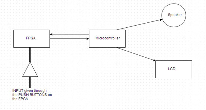
System architecture:

Fig. 1: FPGA-based hardware software co-design overview
Required components:
1. Nexys 2 Spartan 3E FPGA Board
two. Microcontroller – Atmega16 + LCD
3. 8 ohm speaker
4. Connectors
5. CI 74LS245
Construction:
A. FPGA
· The FPGA needs to be configured to receive user input through its input switches (or button switches).
· So the first step is to configure some switches as input to the FPGA.
· Next, we need to make sure that each key corresponds to a different entry. Therefore, we will provide a code (4 bits) to uniquely identify each entry.
· As this is a prototype, we will only define 4 inputs. And therefore code them as:
One => “0001”
B => “0010”
C => “0011”
E => “0100”
· That is, as soon as a switch is pressed, we identify it using the 4-bit code unique to it.
· The next thing to be done by the FPGA is to send these 4 bits to the microcontroller.
· Communication:
Communication can be Synchronous or Asynchronous.
If you prefer asynchronous mode, parallel transmission is the fastest mode to choose.
If you prefer Synchronous mode, I recommend configuring SPI between the FPGA (master) and the microcontroller (slave).
Here I will use Asynchronous Parallel Transmission.
· For transmission, we will use Peripheral Connectors (PMod Connectors) on the Spartan 3E board. The figure below explains this in detail.

Fig. 2: Nexys2 Pmod Connector Circuit Diagram
· We can configure PMods as Input and Output. Here they will be defined as output.
B. Microcontroller
· This unit mainly has two tasks. First, displaying the character on the LCD. Second, play the sound corresponding to the character on the speaker.
· Task 1: Show
Since we are using parallel communication, each of these transmission lines is connected to the corresponding input pins on the microcontroller. Now, there can be two ways to ensure that the data is read correctly;
1. Pins are continually polled to check for any activity. Once there is, the value is read and stored in a variable.
two. We set up an interrupt. This interrupt is triggered from the FPGA when the transmission lines are going to send the bits. Once the interrupt is received, the value is read and then stored in the variable.
· The 2nd method is more efficient than the 1st method. So let's get on with it.
· Therefore, the value is read using the PIN variable
· Task 2: Sound
We have to play a sound on the 8” speaker. For this, we will use the microcontroller's internal flash. We will store a sample sound (say a beep) in memory. And we will play it according to the input. That is, 'A' means playing the beep once. 'B' means touch it twice, and so on.
The microcontroller we are using here is the Atmega16 which has only 16K Bytes of internal flash. Therefore, we cannot store many different sounds in this memory. To achieve this, we need to use an external flash and interface it with the microcontroller. This isn't the focus here, so we won't go there.
And To play PCM audio on the AVR microcontroller, we will use the high-speed PWM (fast PWM mode) of the AVR. It almost looks good and can be used for simple projects that require sound effects.
Step 1: Create a .wav file. If you don't have any, use the following link and convert text to speech. Save it as a .wav file.
http://www2.research.att.com/~ttsweb/tts/demo.php
Step 2: Convert the created wav file to an 8-bit unsigned 8,000 samples per second wav file using NCH's software option. It can be found here:
Step 3: Convert the 8-bit wav file to a sample c file using the software below.
Step 4: Copy the created samples into the pcm_sample header file and save it.
In essence, what we are doing here is taking a sound sample and then sampling it to create finite samples (8000) of 8 bits each. These samples are stored in flash using the PROG_MEM command (due to the use of the avr/pgmspace library). These samples will act as the duty cycle for the PWM that will be generated. We set the initial duty cycle (value in the OCR1A register) to 0. After that, samples will be continuously read from the flash and written to the OCR1A. Finally, the speaker will be connected to the PWM output (OC1A) and we will be able to hear the sounds.
To use the internal flash, we use the following functions:
1. const long pcm_length=6800;
const unsigned char pcm_samples PROGMEM ={ insert samples here };
This function is used to create the “pcm_sample” header file that will be used later.
two. pgm_read_byte(&pcm_samples(sample++));
This function is used to read byte after byte from the header file.
Connections:
For the FPGA:
1. The 4 slide switches SW0, SW1, SW2 and SW3 will be used as input.

Fig. 3: Table listing PMod connectors
two. Next, for FPGA output, we will use PMod JA. The connections are:
Interrupt (O) is connected to JA1 “L15”
Transmission Line “Z0” connected to JA2 “K12”
Transmission Line “Z1” connected to JA3 “L17”
Transmission Line “Z2” connected to JA4 “M15”
Transmission Line “Z3” connected to JA7 “K13”
Note 1: We cannot use JA5, JA6 as they are predefined to be used as GND, VCC.
Note2: Since Spartan 3E works on 3.3V Logic and Atmega16 on 5V Logic, we need to connect a Logic Shifter IC like 74LS245 to level the transmission lines before connecting them to the PORT of the microcontroller.
For the microcontroller:
1. First connect the interrupt to PD2 (since we are using INT0, it can be anything depending on your choice). Then connect the transmission lines to pins 0-3 of any port. Here Port B is used.
two. Connect the speaker through a low-pass filter (resistor (1k) + capacitor (470uf) connected to GND) to PD5 (OC1A-PWM output).
Working:
It can be seen that as soon as we press a button on the FPGA, we can see the corresponding letter on the LCD and hear the number of beats on the speaker.
Conclusion:
This was a simple experiment to show the concept of Hardware-Software co-design. Although this project alone does not explore the full potential of this concept, it is a good start for beginners who can learn from it and use it in their own projects.
Pin Diagrams:

Fig. 4: Image of the 4-slide switch on the FPGA board
74LS245
Project source code
 ###

 // Program to use external interrupts (hardware) from the AVR microcontroller (ATmega16)


Questions related to this article?
 Ask and discuss on the Electro-Tech-Online.com and EDAboard.com forums.
Tell us what you think!! Cancel reply
You need to be logged in to post a comment.