During the semiconductor chip manufacturing process, it is necessary to employ slicing techniques to cut wafers. However, traditional diamond cutting and grinding wheel cutting can cause significant damage to semiconductor materials, leading to problems such as wafer fragmentation and chip performance degradation.
Consequently, the development of advanced cutting technologies has immense importance for reducing costs and increasing efficiency in the integrated circuit semiconductor industry. With the progress of laser technology, high-power laser ablation cutting (i.e. laser cutting) and stealth cutting achieved using low-power focused lasers are gradually becoming mainstream chip cutting technologies.
Laser cutting is a non-contact processing method that, unlike traditional diamond and grinding wheel cutting, prevents chip breakage, tool wear, water pollution, thermal effects and chip entrapment, which are significant problems.
However, the high-power lasers used in laser ablation cutting generate substantial thermal effects during operation, which can easily damage the blue film on the bottom during wafer cutting, thus impacting the chip processing technique. Therefore, stealth cutting technology has gradually become a focal point in the semiconductor manufacturing industry.
(a) Diamond blade cutting (b) Grinding wheel cutting (c) Stealth Dicing (SD) Technology
Advanced Dicing: Detailed explanation of Stealth Dicing technology and illustrative applications
Stealth Dicing technology, by focusing a laser to form a small area of light spot, can generate enormous energy density, thus achieving wafer cutting.
As a dry process, Stealth Dicing offers advantages such as high speed, high quality (no or very few chips) and low cutting loss. The specific Stealth Dicing process can be divided into two steps:
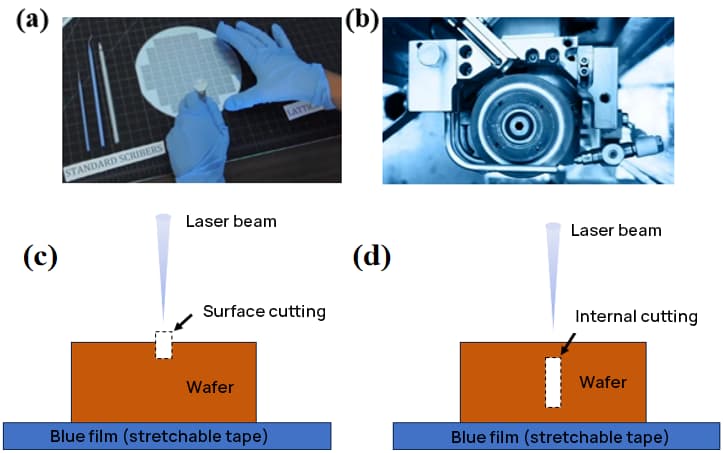
(1) Laser-induced drilling: As shown in Figure 2, a pulsed laser beam that can pass through the wafer is focused below the surface of the wafer by the optical system. When the laser power density at this focus point reaches its peak, a perforation is formed, and at this point the wafer chips are not yet separated.
(2) Chip separation: After unfolding the blue film placed on the wafer, due to the large tensile and compressive stresses present near the laser perforation, cracks can be induced along the laser path inside the wafer, achieving chip separation .

Stealth laser cutting technology has now been applied to a variety of wafer cutting scenarios, such as:
(1) Silicon wafer cutting: When using conventional diamond blades to cut silicon, the blade thickness, granularity, rotation and cutting speed significantly affect the cutting quality. Despite years of technical improvements, the large cutting width (cut) caused by the blade still leads to material waste.
Additionally, debris generation and blade wear increase cutting costs. However, using stealth laser cutting technology with an ultra-narrow cutting path can eliminate the cost issues associated with additional cleaning of debris and material waste, thereby improving chip productivity. Furthermore, by preventing thermal damage, stealth laser cutting technology can further increase chip manufacturing yield.
(2) Silicon carbide cutting: Silicon carbide is an ultra-hard material, second only to diamond in hardness, making it extremely difficult to machine. In the preparation of large size (6 inches and above) silicon carbide crystal substrate materials, stealth laser cutting technology, compared with fixed abrasive wire cutting technology (diamond electroplated steel wire) , can improve cutting efficiency by 3 to 5 times.
Given the significant issue of material consumption, stealth laser cutting technology can also increase the production rate of silicon carbide wafers by more than 30%.
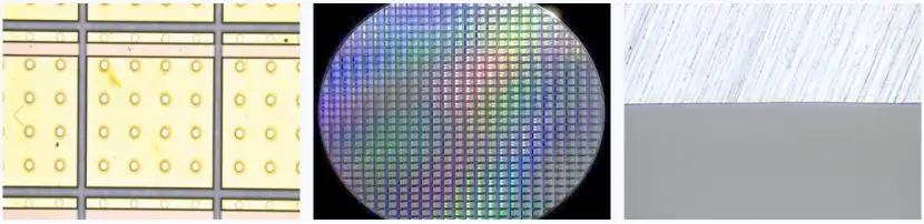
(3) Special wafer cutting: By using stealth laser cutting technology to cut special wafers (for example, wafers with thin films mounted on chips or made of low-k materials), it is possible to avoid the generation of fractures and cracks, achieving high efficiency and high precision wafer cutting.
Advances in Stealth Laser Cutting Technology
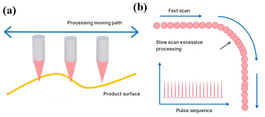
Despite the many advantages of stealth laser cutting technology, a number of problems still interfere with the cutting process. As shown in Figure 4, wafer surface warpage and problems managing laser power density can prevent the laser focus from landing accurately on specific thin layers within the wafer, hindering improvements in cutting accuracy and rate. chip yield.
Due to the difficulty in evenly applying the laser beam during the acceleration, deceleration and turning stages, overprocessing problems can easily occur. Additionally, issues such as analog interference, analog nonlinearity, analog drift, or delays in the driver current loop will affect the control accuracy and responsiveness of the laser cutting platform.
In response to these issues, academic and industrial sectors have proposed a number of solutions, as shown in Figure 5, which specifically include:
(1) Real-time height tracking control: During the wafer cutting process, displacement sensors are used to measure minute height fluctuations on the product surface in real time, and these are compensated in real time for the Z axis where the laser is located, ensuring that the laser focus accurately hits a specific thin layer of the wafer.
(2) High-speed position comparison output control: The development of a height tracking algorithm effectively avoids excessive machining problems during laser acceleration, deceleration and turning, ensuring that the laser acts uniformly on the workpiece.
(3) PWM (Pulse Width Modulation) control technology: By directly outputting digital switching signals from the controller, which are then amplified through a power amplification module to directly control the motor current circuit, an improvement Faster and more direct laser cutting platform control accuracy and responsiveness are achieved.

Regarding the small action area and power adjustment problem of single-focus laser stealth cutting, multi-focus laser stealth cutting technology has been specifically developed. This technique can simultaneously focus and generate multiple focal points within the wafer for cutting, significantly increasing cutting efficiency, as shown in Figure 6.
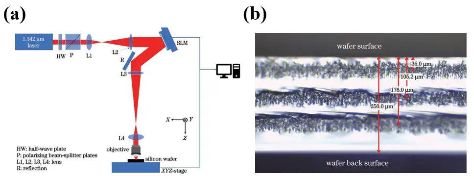
During the multifocal laser stealth cutting process, the position and intensity of the laser beam greatly influence the cutting quality. Due to the significant difference in refractive indices between air and semiconductor materials, the laser beam acting inside the wafer can cause a focal spot scattering phenomenon, thus requiring aberration correction.
To meet wafer cutting needs in various application scenarios, people have addressed these issues through technical advancements such as regulating the position and intensity of multiple foci and developing aberration correction technologies to overcome spot dispersion. focal.
Stealth Laser Cutting Technology: A World of Greater Potential
Compared with traditional cutting technologies, laser stealth cutting has notable advantages in practical applications, including significantly higher efficiency, superior quality and lower loss.
By further optimizing and exploring laser stealth cutting technology, for example, adjusting the beam energy during the stealth cutting process to obtain surface roughness of the photonic chip or increasing the efficiency of laser stealth cutting, we firmly believe that this technology will shine brightly in the field of integrated circuit semiconductor manufacturing as well as other emerging domains.