The term transistor is derived from the words “transfer and “resistor”. The first semiconductor transistor was invented to replace the triode as an amplifier device, a vacuum tube with three electrodes. The transistor was smaller, lighter and cheaper than a tube triode. It also proved to be easy to build and had no heat losses like a triode.
A little of history:
- The first transistor was a point contact transistor developed by John Bardeen, Walter Brattain and William Shockley in 1947 at Bells Lab.
- In 1948, the first bipolar junction transistor was developed by William Shockley.
- In 1951, the first commercial transistor radios were introduced.
- In 1954, the first integrated circuit was developed by Jack Kilby at Texas Instruments using transistors.
Since then, transistors have been a cornerstone of electronics, providing an important part of digital circuits for power electronics.
Bipolar junction transistors (BJT) are the most common type. A BJT is similar to two semiconductor diodes combined into a three-terminal device and is also made from semiconductor materials such as silicon and germanium. A transistor is typically used to amplify or switch electronic signals.
A BJT has three terminals:
- The base is the control terminal
- The collector and emitter are the input/output terminals
As its name suggests, a BJT is a bipolar electronic device. This means that both electrons and holes participate as charge carriers. The term “junction” indicates two PN junctions in a bipolar junction transistor. The term “transistor” refers to its function as a signal amplifier. A small current applied to its base controls the much larger current between the emitter and collector.
BJT is a fundamental electronic device, widely used in electronic circuits for signal amplification, switching and processing. It is versatile and is found in a variety of applications, including digital integrated circuits, oscillators, signal processors, and power electronics.
In this article, we will discuss the basic concepts of a bipolar junction transistor and explore its practical uses in circuits.
What is a BJT?
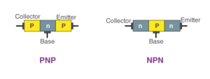
A bipolar junction transistor (BJT) is a three-layer semiconductor device consisting of two p-type layers, one n-type layer, or two n-type layers and one p-type layer.
- A transistor that consists of two n-type layers and a p-type layer sandwiched between them is called an NPN transistor.
- A transistor composed of two p-type materials and an n-type layer sandwiched between them is called a PNP transistor.
These transistors are named based on the arrangement of their semiconductor layers and the majority of charge carriers involved in their operation.
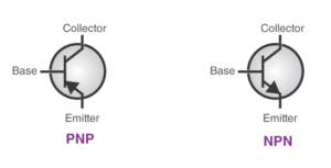
The symbols for NPN and PNP transistors are shown below.
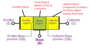
BJT Construction
A transistor is similar to a triode and is used to amplify signals. In a transistor, the emitter layer is heavily doped, while the base and collector are lightly doped.
The emitter and collector are much wider than the base. The ratio of base width to total transistor width is typically 150:1. The doping level of the base layer is also 10 times lower than that of the collector and emitter. Due to lower doping levels, the base has limited free charge carriers, resulting in greater resistance.
How a transistor works
Just like a semiconductor diode, a transistor also requires proper biasing to function. Biasing refers to setting the DC operating conditions of the transistor so that it operates in a desired region.
Like a semiconductor diode, the output characteristics of a transistor are divided into distinct regions. Proper biasing for NPN transistor is shown below.

To understand how a transistor works, think of it as two PN junctions – one between the emitter and the base and the other between the base and the collector.
Suppose the base-collector junction is assumed to be open (due to the negative potential at the N-type emitter and the positive potential at the P-type base). In this case, the emitter-base PN junction is forward biased.
In an N-type emitter, a heavily doped transistor region, electrons are the majority charged carriers. Due to forward bias at the emitter-base junction, a large number of electrons flow from the emitter to the base, while a small number of holes pass through the base to the emitter.
Next, let's assume that the emitter-base junction is open. In this case, there is a negative potential applied to the P-type base and a positive potential applied to the N-type collector. As a result, the PN junction of the base collector is reverse biased.
In a reverse bias condition, the current from the minority charges carries the flux from the base to the collector. In the P-type base, electrons are the minority charged carriers, and in the N-type collector, holes are the minority charged carriers.
However, many electrons are also injected from the forward bias of the base-emitter junction. Due to the high resistance of the base region, only a negligible amount of current passes through the base terminal. Most of the electrons injected into the base region diffuse to the N-type collector region.
By applying Kirchhoff's current law to the transistor, we obtain the following equation.
I E = I B + I C
The above current relationship remains applicable whenever a transistor is connected in a circuit. Collector current has two components:
I C = I Majority + I CMMinority
The base current is almost insignificant in terms of the order of microamperes or nanoamperes. The emitter and collector currents are on the order of milliamps.
Since the base current is almost negligible when the base-emitter junction is forward biased and the collector-base junction is reverse biased, the emitter current and collector current are almost equal.
I E =̃ I C
The collector current, due to the minority carriers (i.e., the holes in the N-type collector) is negligible due to the high resistance of the base region.
Thus, we can say that the emitter current and the current passing through the collector of the majority carriers (i.e. electrons) are equivalent in the case of the NPN transistor.
I E =̃ I Majority
Thus, for any voltage between the base-collector junction, the current passing through the collector is equivalent to the current in the emitter. The DC bias at the base of the transistor controls the flow of current from the emitter to the collector. A PNP transistor operates in the same way, except that the roles played by electrons and holes are swapped.
In an NPN transistor, the current between the emitter and collector comes largely from the flow of electrons from the emitter to the collector. This is why the direction of conventional current is indicated by an arrow pointing away from the emitter.
In a PNP transistor, the current between the emitter and collector is largely due to flow from the emitter holes to the collector. This is why the direction of conventional current is indicated by an arrow pointing into the emitter.
Features VI
As a three-terminal device, the BJT has an input side and an output side. One of the terminals remains common between the input and output sides. This terminal is also closer to or at ground potential.
The VI characteristics of a BJT are then divided into two sets of characteristics: the input parameters or trigger point and the output characteristics.
Now suppose the transistor is connected in such a way that the base terminal is shared between the input and output sides. This is a common base configuration of the transistor. The input signal is applied to the emitter and the collector receives the output signal.
Because the input side must be forward biased for any current to flow between the emitter and base, the input VI characteristics are similar to the forward bias characteristic curve of a diode. The input characteristics of the BJT in a common base configuration are shown below.
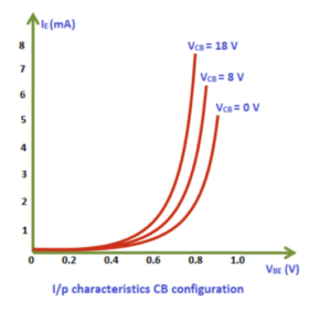
As can be seen from the input characteristics curve for common base configuration, if the base-collector voltage is constant, the emitter current (input signal) increases exponentially after a certain base-emitter voltage.
If the collector-base voltage increases, the exponential rise starts earlier and the emitter current increases to a higher value for the maximum voltage allowed at the collector-base junction.
The output characteristic curve for the common base configuration is shown below.
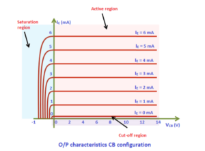
The collector current (output signal) has three distinct regions of operation compared to the base collector voltage. When the base-emitter and base-collector junction are reverse biased, the emitter current and collector current are zero.
There is negligible current flow in the collector due to minority carriers, which can be ignored. This is the cutoff region of the transistor. In this region the transistor is turned off. There is no base current or collector current.
When the base-emitter and base-collector junction are forward biased, the collector current increases sharply for a slight change in the base-collector voltage. This is the saturation region of the transistor. In this region, the transistor is fully turned on and a maximum collector current flows. This region of operation is useful for using a transistor as a switch or for building logic gates.
When a base-emitter junction is forward biased and the base-collector junction is reverse biased, the collector current approaches the emitter current and there is no effect or change in the collector base voltage on the collector current. This is the active region of the transistor. In this region, the transistor operates as a linear amplifier. A small base current controls a larger collector current, allowing signal amplification.
An NPN transistor is formed by sandwiching a P-type region between two N-type regions. Electrons are the majority carrier.
To operate an NPN transistor in an active region, a positive voltage is applied to the collector (VCC), and a more positive potential is applied to the base terminal relative to the emitter terminal (VBE).
In the active region, electrons flow from the emitter to the collector in an NPN transistor, resulting in a conventional current flowing from the collector to the emitter when a small current flows from the base to the emitter.
A PNP transistor is formed by sandwiching an N-type region between two P-type regions. The holes are the majority carriers. To operate a PNP transistor in the active region, a negative voltage is applied to the collector (VCC) and more negative potential is applied to the base terminal compared to the emitter terminal (VBE).
In the active region, holes flow from the emitter to the collector in a PNP transistor, resulting in a conventional current flowing from the emitter to the collector when a small current flows from the emitter to the base.
NPN transistors are easier to manufacture and typically have better performance characteristics, such as higher current gain (β). They are often used in low-side switching applications, amplification circuits, and as active components in digital logic gates.
PNP transistors are less common than NPN BJTs, but are essential for certain circuit configurations. They are used when the circuit design requires a different polarity or when the power supply voltage is negative with respect to the ground reference. PNP transistors are often used in high-side switching applications, motor control, and as active components in complementary digital logic gates.
In some applications, NPN and PNP BJTs are used together in a complementary pair configuration. This pairing allows amplification and switching of positive and negative signals, making them suitable for applications such as push-pull amplifiers and complementary symmetry power amplifiers.
Three BJT configurations
BJT has an input side and an output side when connected in a circuit. One of the transistor terminals remains common between the input and output.
There are three possible configurations for connecting a transistor in a circuit.
1. Common Base (CB) Configuration: The base of the transistor is common between the input and output sides of the transistor. The input is applied to the sender terminal and the output is connected to the collector terminal. This configuration is not as common as the CE configuration, but is used in some specialized applications, such as high-frequency amplifiers.
In this configuration, the output signal is in phase with the output signal. CB offers current gain as a small change in emitter current results in a larger change in collector current. The voltage gain remains less than '1', so the output voltage is less than the input voltage. The configuration has low input impedance and high output impedance. This is why it is used for impedance matching rather than voltage amplification.
2. Common Emitter (CE) Configuration: The emitter is the common terminal between the input and output sides. The input is applied to the base and the collector gets the output signal. This is the most common configuration for BJT.
In this configuration, the output signal is 180 degrees out of phase with the input signal. CE offers high voltage gain and moderate current amplification. The input impedance is moderate, while the output impedance is relatively high. Because the common emitter configuration provides voltage and power amplification, it is used in audio amplifiers and signal processing circuits.
3. Common Collector (CC) Configuration: The collector is the common terminal between the input and output sides. The input is applied to the base terminal and the output signal is obtained at the collector terminal. This configuration is also not as common as the CE configuration.
In the DC configuration, the output is in phase with the input signal and closely follows the input signal with only a slight voltage drop. However, this configuration still offers high current gain and is commonly used in current amplifiers. The configuration has high input impedance and low output impedance.
Transistor bias
Biasing a transistor refers to the process of defining the DC operating conditions of the transistor so that it operates in a defined operating region, active, saturation, or cutoff. For amplification, the transistor must operate in the active region. To act as a switch in a circuit, the transistor must operate in the cutoff and saturation regions.
Biasing involves defining the quiescent point (Q point) or operating point of the transistor. This point sets the DC voltage and current levels when no AC signal is applied. The Q point is essential to ensure that the transistor operates within its active linear region for amplification or switching applications.
When biased to operate in the active region, the bias maintains the stability of the transistor and prevents it from entering saturation or cutoff when subjected to various environmental conditions or signal variations. It ensures that the transistor remains in the linear region required for amplification.
The process typically involves selecting appropriate resistor values and DC voltage sources in the transistor circuit to set the transistor base current and establish the collector current at desired levels. It is important to consider several factors, including transistor characteristics, temperature variations, and desired output characteristics.
There are several biasing techniques used in bipolar junction transistors such as fixed bias, emitter bias, voltage divider bias, emitter follower, and collector feedback.
A circuit
When a transistor is connected into a circuit, proper biasing is the first thing that must be addressed. If the transistor is used for amplification or switching of high currents, a suitable heat sink must be used to prevent any thermal damage.
In switching applications, BJT may also require protection against voltage spikes and reverse currents using flyback diodes or other techniques.
Forms
BJTs are used in a variety of applications in electronics. Some of the common applications are as follows.
Amplification: BJTs are commonly used for current or power amplification. They can amplify weak input signals, making them stronger and suitable for further processing or transmission. Typical amplifier applications for BJTs include audio amplifiers, RF (radio frequency) amplifiers, and instrumentation amplifiers.
Switching: BJTs are excellent electronic switches. When properly biased and brought to saturation (ON state) or cutoff (OFF state), they can control the flow of high current loads. This makes BJTs ideal for applications such as digital logic gates, power switches, and pulse width modulation (PWM) controllers.
Voltage Amplification: BJTs are used to build operational amplifier (op-amp) circuits, which provide high voltage gain and are essential in diverse analog signal processing applications such as amplifiers, filters, and instrumentation.
Audio Applications: BJTs have an excellent ability to accurately amplify audio signals. This is why they are often used in audio applications such as microphone preamps, amplifiers, and equalizers.
RF Applications: BJTs, like RF amplifiers and mixers, are commonly used in RF circuits. They process and amplify high-frequency signals for wireless communication and transmission.
Signal Processing: BJTs are used in signal processing circuits such as filters and signal modulators. They help shape, filter, or modify signals in applications such as audio processing, communications systems, and equalization circuits.
Digital Logic Gates: Although FETs are more commonly used in digital logic circuits today, BJTs have historically been used to construct logic gates such as NOT, AND, OR, and NAND gates.
Voltage regulation: BJTs can help maintain a stable output voltage regardless of variations in input voltage or load conditions. This is why BJTs are used in voltage regulator circuits.
Current sources and sinks: BJTs can be used to create precise current sources or sinks. They are useful for biasing other transistors or providing stable reference currents for sensors and measurement circuits.
Light detection: Phototransistors are a specialized type of BJT, used in light sensors, optical switches, and detectors to convert light into electrical signals.
Temperature Sensor: BJTs are used as temperature sensors in temperature compensation circuits.
Oscillation: BJTs are vital components in oscillator circuits, which generate periodic waveforms. Oscillators are used in radios, signal generators, and clocks to produce accurate and stable frequency signals.
Motor control: BJTs drive motors and control their speed and direction in motor control circuits. These transistor circuits are used in robotics, electric vehicles, and industrial automation applications.
The bipolar junction transistor is a versatile electronic device. Engineers and designers rely on BJTs to perform a variety of functions, from signal amplification to power control, making them essential in many electronic devices and systems.
Commercial BJTs
Bipolar junction transistors are versatile electronic devices used in many electronic applications. There are many types of commercial BJTs available on the market.
Circuit engineers and designers choose the appropriate type based on the specific requirements of their circuits and applications, considering factors such as voltage, current, frequency, power handling capabilities, and specific circuit needs.
Some of the most common types of commercial BJT are as follows.
1. Small Signal NPN/PNP BJTs: General purpose transistors used for small signal amplification and switching applications. Examples include 2N3904 (NPN), BC547 (NPN), 2N3906 (PNP), and BC557 (PNP) transistors.
2. High-frequency BJTs: Operate at high frequencies and are often used in radio frequency (RF) amplifiers and other high-frequency applications. Examples include transistors 2N2222 (NPN), 2N3866 (NPN), 2N2369 (NPN), 2N2907 (PNP), and 2N5179 (PNP).
3. High-frequency RF BJTs: Optimized for extremely high-frequency applications such as microwave amplifiers and communication systems. Examples include transistors 2N3866 (NPN), 2N5109 (NPN), 2N2219A (NPN), 2SC3355 (NPN), 2N2907A (PNP), and 2SC2999 (PNP).
4. Power BJTs: capable of handling higher levels of current and power. They are used in power amplifiers, voltage regulators and high current switching applications. Examples are the power transistors 2N3055 (NPN), MJE13009 (NPN), BD139 (NPN), TIP31 (NPN), MJ2955 (PNP), 2N6107 (PNP), 2SA1943 (PNP) and TIP32 (PNP).
5. High Voltage BJTs: Support higher voltage levels and are used in applications that require high voltage amplification or switching. Examples include 2N3773 (NPN) and MJ10012 (PNP) transistors.
6. Low Power BJTs: Operate at low power levels, making them suitable for battery-powered or energy-efficient applications. Examples are 2N3904 (NPN), 2N2222 (NPN), PN2222 (NPN), 2N4401 (NPN), BC547 (NPN), BC109 (NPN), 2N3906 (PNP), 2N2907 (PNP), PN2907 (PNP), 2N4403 (PNP ). ), transistors BC557 (PNP) and BC179 (PNP).
7. High gain BJTs: have extremely high current gain (β) and are used in applications where signal amplification is critical, such as high frequency RF circuits. Some examples include 2N3904 (NPN) and BC547 (NPN) transistors.
8. Darlington BJTs: consist of two BJTs connected in series, providing very high current gain (β), and are used in applications that require high current amplification, such as power drivers. Examples include the Darlington TIP120 (NPN), TIP122 (PNP), and TIP125 (PNP) transistors.
9. Switching BJTs: designed for fast switching applications, often used in digital circuits and pulse width modulation (PWM) applications. Examples include transistors 2N2369 (NPN), 2N3906 (NPN), 2N4401 (NPN), 2SC945 (NPN), and 2SC945 (PNP).
10. Low noise BJTs: designed to have minimum noise characteristics and used in sensitive electronic circuits such as low noise amplifiers for radio receivers. Examples are transistors 2N2222A (NPN), 2N4403 (NPN), 2N5109 (NPN), BC549C (NPN), BC550C (NPN), 2N3906 (PNP), BC560C (PNP), 2N4401 (PNP) and BC560C (PNP).
11. Audio BJTs: Designed for audio amplification applications such as audio amplifiers and preamplifiers. They feature low noise and low distortion characteristics. Examples are 2N3904 (NPN), 2N4401 (NPN), 2N2222A (NPN), KSC1845 (NPN), BC546B (NPN), BC547C (NPN), 2N3906 (PNP), 2N4403 (PNP), 2N2907A (PNP), KSA992 (PNP ). ), BC556B (PNP) and BC560C (PNP) transistors.
12. Phototransistors: sensitive to light and commonly used in optoelectronic applications such as light detectors and optical switches. Examples are the transistors TEPT5700 (NPN), PT334-6C (NPN), PT204-6B (NPN), BPW34 (NPN), TSHA4400 (PNP), TIL194 (PNP) and PT138 (PNP).
Temperature Compensated BJTs: Provide stable performance over a wide temperature range and are used in applications where temperature variations are a concern.
Surface Mount (SMD) BJTs: Available in compact surface mount packages, making them suitable for modern PCB assembly techniques.

