By Arshon Technology
For PCB prototype applications, one prerequisite is mandatory: reliable testing. These first products are built for the sole purpose of testing design ideas to ensure they work for approved use and sale. Be that as it may, PCBs can be unpredictable as there are many parts and patch associations.
When electronic circuits were more basic and straightforward, manual visual examinations (MVI) were adequate to identify possible problems such as short circuits, overloading, faulty joints, broken parts, missing components, etc.
However, MVI was also subject to human error and oversights and could be an exhausting and tedious task. This has led to circuit imperfections and excessive and unnecessary costs due to failures or recalls.
 Since then, the PCB manufacturing industry and PCB-related manufacturers have established various testing and evaluation techniques to ensure safe and reliable products. Current testing standards better identify faulty circuit components where current or future failures may occur.
A testing process roboticizes visual examination using an automated optical inspection (AOI) method. AOI typically uses a camera that autonomously checks a PCB device to test for quality, missing parts, and potential failures. It is now widely used during pre- and post-flow welding and accessible on some pick-and-spot machines.
As surface mount devices (SMD) and spherical grid array (BGA) packages — a type of surface mount package or chip carrier used for integrated circuits — have become more common, the limitations of AOI for testing have become more apparent. Unfortunately, AOI often cannot identify the welds that are under the beams.
As a result, an automated X-beam inspection (AXI) method was developed, which can reveal hidden PCB assembly defects even in the thickest and most multifaceted components of a PCB. As PCBs have evolved, so have testing methods to ensure reliability.
Upon completion of this initial assessment step, PCBs will typically undergo exact specification testing, performed on the entire assembled circuit.
What are the main components analyzed during PCB prototype testing?
When a PCB prototype is tested, it means the board's circuit design is evaluated to ensure it is safe and suitable for your project. The circuit is a combination of electronic components that will be connected by conductive wires within the final PCB design and through which electrical current can flow.
These electronic components may include:
- Capacitors (C)
- Resistors (R)
- Diodes (D)
- Fuses (F)
- Inductor (I)
- Integrated Circuit (IC)
- Transistor (T)
- Reread)
These are the components that require testing to detect any faults or irregularities that could lead to PCB failure. It is also important to ensure that they are of the ideal type and quality for the project in question.
For example, it is important to consider anticipated environmental conditions (such as temperature and humidity) as well as available current. Ask yourself: in the event of a short circuit, overload or overheating, what will happen?
Let's review some of the testing methods available.
PCB Testing Methods
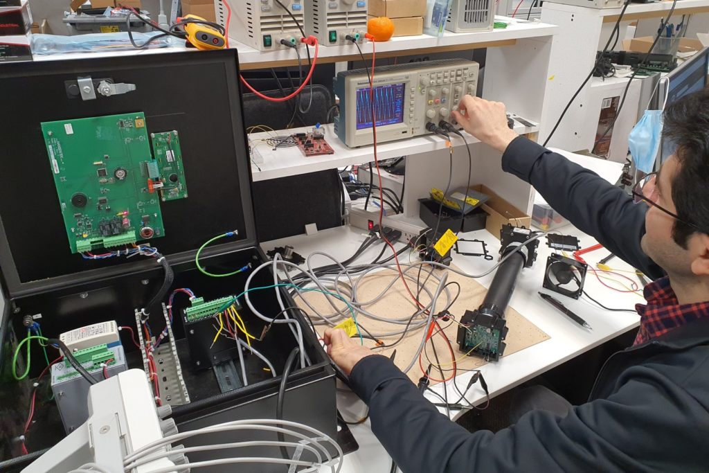
In-circuit testing: One of the most ideal tests for PCB prototype evaluations is in-circuit testing (ICT). It provides a reliable method of checking high fault coverage of all electronic components in a PCB assembly. The TIC works by controlling and inciting the PCB hardware and aims to give 100% inclusion. The advantage is that it completely eliminates the chance of human error.
Test steps:
- Place the probes fixed
- Check the connections
- Start the test
Access the mounting points on the printed circuit board and make sure it is solid by applying a little tension to it.
Ideal for:
- BGAs or main assemblies – and after the assembly is complete.
Short Circuit Test: This test requires checking the resistance between different points in the circuit. A multimeter can be used. Many PCBs are damaged due to short circuit currents.
It is important to focus on fine-pitch parts, such as microcontrollers with LQFP printing. This is because a solder wire that causes a short circuit between two adjacent pins can completely damage and ruin the microcontroller. Be sure to measure the impedance of each different voltage hub relative to ground.
For example, there may be a 12, 5, and 3V power network on a PCB, and any of them may be shorted due to poor fixing or broken parts. This may cause parts to heat up when turned on.
Flying Probe Testing: A practical technique that tests PCB probes from one point to another (hence the name “flying”), requiring ICT power. This test is very cost-effective for prototyping and low to medium volume production as no custom fixtures are required.
It is typically used to look for unique problems in the circuit, such as:
- Shorts
- Capacitance
- Resistance
- Inductance
- Open
- Diode Problems
Test steps:
- Connect the needles to a test on an xy grid (taken from AUTOCAD FILE)
- Probes can be moved around the circuit board to evaluate alternative points or individual parts
Reverse Polarity Test: Reverse polarity happens when a receptacle is plugged in backwards. If you have reversed one or two wires in the circuit, there is usually no return. You will be greeted with a popping sound and a small haze of smoke. In simple cases, you can remove the damaged parts without replacing the entire board.
To protect the PCBs from the effects of reverse polarity, it is possible to insert a protection diode. However, a diode consumes power.
Automated Optical Inspection (AOI) Testing: A primary visual method used to check for any obvious or emerging issues or concerns in the underlying phase of an assembly using a camera.
Test steps:
- Take images of circuit board parts for testing
- Compare images with a detailed schematic
- If the board coordinates with the schematics for a specific rate, the test passes
Ideal for:
- Detect initial problems that may occur on the board during the assembly cycle. It is advisable not to rely solely on AOI for thorough testing. Add a TIC or flying probe method for more reliable results.
Burn-in test: involves passing a power supply through the electronic components of a PCB, typically at an elevated temperature – or at its specified maximum capacity. Its usefulness is found in construction and testing of load limits. But care must be taken because testing can put PCB components at risk. Ideally, burn-in early and/or when the cost of testing and replacing parts is low.
Test steps:
- Pushing high power through the PCB, typically to its extreme limit.
- Power can pass through the board for 48 to 168 hours
- If the advice fails, this is known as “infant mortality”.
Ideal for:
Note that this test is not ideal for PCBs in all conditions. Burn-in testing can decrease the longevity of a PCB. Therefore, it should only be used when necessary and not uselessly.
It may be useful for:
- Test an item as much as possible before releasing it
- Early discovery of an underlying problem during assembly
Testing Filled Components: It can be frustrating to spend hours investigating why the microcontroller won't turn on, only to realize that the gem oscillator's stack capacitor has not filled. But when there are multiple parts to consider, it's easy to miss a component or two. When working with a PCB prototype, you first want to ensure that the components are suitable for the circuit board you plan to design.
Before you start checking each component, make sure you use the correct bill of materials.
X-ray inspection test: An X-ray can locate defects early in the assembly process that are undetectable to the human eye, such as those under the chip package. There are 2-D and 3-D AXI tests, with the latter offering a faster testing period for the PCB prototype.
Tested for:
- Solder Connections
- Barrels
- Internal tracking
Ideal for:
Note that, similar to burn-in testing, X-ray inspections can decrease the longevity of a PCB, so only test when the benefits outweigh the cons, such as when:
- Inspect layers of plaque that cannot be seen without an x-ray
- When a trained technician is available
Functional Testing (FCT): Typically simulates the operating environment of the product under test and is performed as the last step before final manufacturing. Parameters are usually provided by the customer and may depend on where the PCB will be used. Often, a computer is connected to the test points to determine whether the PCB meets its intended capabilities.
Prerequisites for testing :
- Provided by customer
- May include requirements for UL, MSHA or other standards
- Includes accessories or external equipment
Ideal for:
- The last test before sending the item
- Quality assurance, but can be time-consuming
Additional PCB Tests
There are several types of tests other than those mentioned above, depending on the circumstances.
Other tests:
- PCB contamination test: identifies ionics on the board that can cause contamination
- Weldability Test: Used to check surface plate durability and ensure reliable solder joints
- Microsection analysis: detects defects, failures, shorts or faults
- Peel test: finds the amount of energy needed to peel the laminate from the board
- Time domain reflectometer: used to identify flaws in high-frequency boards
Ideal for:
- Reducing customer support
- Use with different tests like ICT or flying probe for extra guarantees
- Identifying faults
Before deciding on the ideal test for your project, determine the purpose of the PCB. Weigh the pros and cons of the different tests available, including their costs. Sometimes you may want to perform more than one test. Often, your electronics contract manufacturer will help you identify what is best to do.
REFERENCES
- Functional Testing of PCBs, Assembly Magazine, Adam Cort, July 1, 2002
- ICT, In-Loop Testing Tutorial — notes and details on all the basics of in-circuit testing
- AXI Automated X-ray Inspection for PCB and BGA – Basics about Automated X-ray Inspection, AXI, systems used for inspection of PCB printed circuit board assemblies and especially those with BGA ICs
- NXP, “Understanding Power MOSFET Datasheet Parameters”, NXP Semiconductors, Eindhoven, 2013
- Maliniak, “Testing is a matter of life and death in the automotive industry,” Electronic Design, October 4, 2011