PCB Basics:
TO NEED:
If we connect different electronic components directly with wires or their conductors, we have to face many problems like loose connection, troubleshooting issues, low reliability, low durability, etc. On the other hand, we may lose connections due to lack of physical support. The only solution to avoid all these problems is “PCB”.

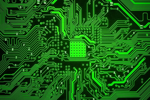
Fig. 1: Image of a PCB layout
PCB:
PCB stands for “Printed Circuit Board”. In this, the wire connections are printed as copper tracks. It can provide physical support to the circuit, thus preventing loose connections. Furthermore, testing and troubleshooting the circuit also becomes simple. We can maintain the size of the circuit so that it can be accommodated in the desired location. Nowadays very complex circuits like motherboards are also designed as PCBs by engineers.
History:
If we look at the history of PCBs, its initial phase was referred to as “printed wire”. 1st patents for “printed wires” were issued in 1900, but PCBs came into use after World War 2. Charles Ducas of the United States filed a patent application for a method of creating an electrical path directly on the insulated surface by printing through a stencil in the year 1925. But in 1943, Dr. Paul Eisler was credited with making the first operational printed circuit. frame. It was used as a replacement for bulky radio tube wiring.
PCB Layers:
The simple printed circuit board contains copper tracks only on one side of its surface. These types of boards are called “One Layer” printed circuit boards. The most common PCBs are 2-layer PCBs, which contain copper tracks on both sides of their surface. It is also possible to design PCBs with more than two layers; these are called multilayer PCBs containing 8 or more layers.
In multilayer PCBs, alternating insulated and conductive layers are laminated together under high temperature and pressure. This process ensures that air is not trapped between the layers and that the conductors are completely encapsulated by resin. The range of material combinations is extensive, from basic epoxy glass to exotic ceramic or Teflon materials. Multilayer PCB manufacturing needs a specialized hydraulic press with heated plates.
Advantages of Multilayer PCBs:
1. Greater flexibility.
2. Considerable savings at a fast pace.
3. High assembly density.
4. Reduces overall weight.
5. Reduces interconnecting wiring harnesses.
Applications of Multilayer PCBs:
1. Where cross-talk levels are critical, multilayer PCBs are very useful.
2. Although the weight and space are considerable, multilayer PCBs are especially valuable.
3. In aerospace PCBs.
4. Manufacture of computer motherboards and mobile boards.
5. Satellite systems.
6. X-ray equipment.
7. Medical electronics. Etc.
Terminology:
| Y.No | Term | Meaning |
|---|---|---|
| 1 | Thousand | One thousandth of an inch (1 mil = 0.001 inch = 25.4 microns) |
| two | Although | Thousandth part of an inch and equivalent to “thousand” |
| 3 | mm | Thousandth part of the meter (millimeter) |
| 4 | ESD | Electrostatic discharge caused by static electricity |
| 5 | Trace | A path made of copper on the PCB. It is the same as a wire used to connect components. |
| 6 | By | It is a hole with copper inside, which can provide electrical connection between the trace of one layer and the trace of another layer. |
| 7 | Cushion | Pads are conductive surfaces for soldering SMD devices. |
| 8 | Annular Ring | It is the area of the cushion that surrounds the track. |
| 9 | silk screen | Markings of names and values of components and outlines on a PCB. This will help in easy assembly and debugging. |
| 10 | solder mask | It is applied to the entire board, except the pads, and is a substance that solder does not stick to. |
| 11 | Surface Finish | A layer on top of the pads to prevent oxidation of the copper layer |
| 12 | Gerber File | The file which is in Gerber format and can tell the manufacturer all the information of the PCB. Such as dimensions, layouts, etc. |
| 13 | Through hole components | These are components that have terminals like normal resistors. The cables for these components are soldered to the other side of the board. |
| 14 | Surface Mount Devices | These are cable-free components that can be simply soldered onto pads rather than through holes. |
| 15 | Panelization | Manufacturers will create a huge PCB with identical boards and often cut into individual boards. This process is called panelization. |
| 16 | PCBA | Printed circuit board assembly consists of soldering components onto the PCB. |
| 17 | FR-4 Substrate | Most commonly used material to create PCBs |
| 18 | CAM | Computer-aided manufacturing |
| 19 | CAM files | These are data files directly used in PCB manufacturing.
Examples: Gerber file, NC drill file, manufacturing and assembly drawings, etc. |
| 20 | Capture | Extract information automatically using software. |
| 21 | Component Library | Representation of components as deculs and used by CAD software. |
| 22 | Connection | Also called “pair of pins”, it is the connection between two points. |
| 23 | Decal | A graphical representation of the component. |
| 24 | GOOD | It stands for “bill of materials”, which provides the list of PCB components. With this we can check the components that we forgot by mistake. |
| 25 | Footprint | Collection of cushions and contour that constitutes an individual component. |
| 26 | Blind way | Via used between the top layer and the inner layer. |
| 27 | Buried via | Via between internal layers. |
| 28 | Through hole via | Via between the upper and lower layers. |
Software tools and procedures:
In the market, many PCB design software are available, such as ORCAD, Eagle CAD, ALTIUM, ULTIBOARD, etc. Alternatively, we can use open source software like KICAD, Free PCB, etc. WEB versions software are also available such as PCBWEB designer.
In any software, the procedure for designing PCB is very similar, but options, components, libraries, quality, and automatic routers are different.
The basic procedure is:
Step 1: Schema creation.
In this, we have to select the components, make their connections and assign values to the components.
Step 2: Switch to the board and modify the board.
After creating the schematic, switch to the board. As output we will obtain components with perfect dimensions and connections. Place these components correctly according to the PCB size, shape, dimension and requirements (placement of components is our choice). Place holes with appropriate drill dimensions.
After this step, apply Automatic Router. It will provide well-routed copper trace PCB output and layout. But sometimes the automatic router cannot route completely; In these cases, we have to edit the traces manually. There is more manual routing in multi-tier design.
Step 3: Generating Gerber files.
After finishing the routing, apply the CAM process to generate Gerber files. In the CAM process we can obtain Gerber files, NC drilling files, assembly drawings, etc. These files will help the manufacturer in preparing the PCB.

