For people who are doing PCB Design For amateurs or professionals, there are many PCB design software available. The most popular among them are diptrace, orcad, eagle, kicad etc. This tutorial is mainly for those people who haven't tried any professional PCB designer software yet.
Here's a quick guide that will help you get started with kiCAD. In this tutorial, we will consider a simple astable multivibrator circuit using timer IC 555. We will be designing a printed circuit board for this well-known simple circuit. Let me say upfront that I am not an expert in printed circuit board design. My intention is just to explain the necessary steps in Kicad to convert a simple circuit diagram into a gerber file, and also some tips and precautions to be taken when doing the project.
I'm here doing a complete design process and at the same time explaining the steps to you with the help of screenshots of the same. I request the reader to perform the same steps on your PC from start to finish for this single example, and next time you can do it yourself.
kiCAD software mainly has the following utilities:
Eeschema – Schematic editor
Cvpcb – Components for modules
Pcbnew – PCB Editor
Gerbview – Gerber viewer
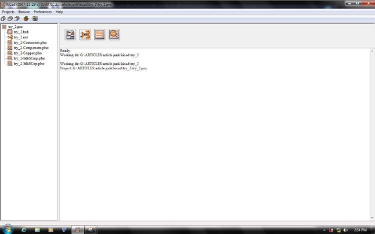
The main Kicad window looks like this:

Your recent project may have been listed in the project tree. To start a new project select “New Project Descr”

The most important thing that you must take care of is that all the files generated while running the project must be saved in a single folder, and the title of all the files must be the same.
So let's save this new project in our projects folder. The extension must be .pro

After saving the project, the main window will look like this:

Editing the Schema
1) Editing the schema
Now you need to convert circuit diagram to schematic in kicad. To do this you need to select the schematic editor.

The schematic editor window is shown below:

Before we start drawing the schematic, we have to do a few important things;
Page Settings – To set page size, title, etc.

Page settings window:
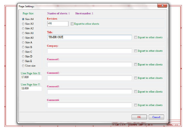
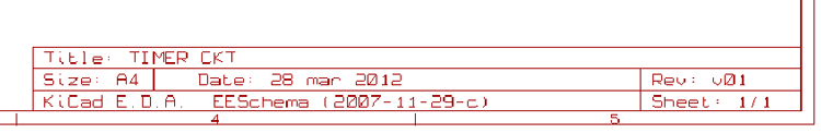
When you press OK, you can see that your worksheet title has changed like this:
Now we need to set the preference

General options window:
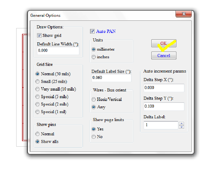
Press OK and save preferences:

To make our design process faster, we need to use a lot of hotkeys. We can have a list of shortcuts currently in use like the following:
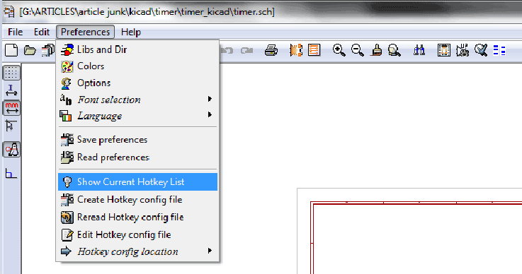
Current list of hotkeys:

Now we have defined most of the necessary things, so we can start drawing the schematic.
It's all about selecting the right component, positioning the component, connecting them and annotating.
First we add all the components. To add a component to the worksheet, press A and the component selection window will open. If you know the component's keyword, simply type the keyword and press OK.
The keyword for resistor is R and capacitor is C, so
Component selection window:

Use the Insert key to add the same component again. Press M to move a component after placing the cursor over it. Use ctrl + scroll to move the entire page left/right, shift + scroll to move the entire page up/down

So far we have added the resistors and capacitors to the schematic, now we have to add the 555 IC, LED and 3-pin connector. If you don't know the component keyword you can use the “via library browser” button, which will list all the components in the library.

After selecting the required component, you can use the export to schematic link to add the component to your schematic.
Selecting 555 IC from the component list:

When you finish adding the specific circuit components, the schematic editor will look like this.

Now we need to make the connections. You can hold the cursor at any point and press W to add a wire.

After finishing the connections, it would be best to add some text labels in the required areas. You can do this using the T button as shown in the figure above.

Now our schematic diagram is almost complete. The next step is to write down the components. We can automatically annotate components using the schematic annotation button. The following window will open.

Press the annotate key to automatically annotate the components.

Our finished scheme will look like this:

For this particular tutorial it's not important whether the circuit is correct or not, all I'm trying to explain is just how to convert your circuit into a printed circuit board.
Now, if you wish, you can do the ERC (Electrical Rules Check) using the “schematic check of electrical rules” button.

Press the “Test Erc” button for the following window:

If there are errors, it means you have violated some rules. Errors will be shown in the schematic using markers and you can easily identify and correct these errors. If you have no idea about ERC, don't worry, it will not affect most of the simple circuits in any way.
Now you must save the schema as the following:

Components for Modules
two) Components for modules
The next step is to generate a netlist of the components using the “Netlist generation” button:

Click the “Netlist” button to the following window:

Save the netlist file using the .net extension:

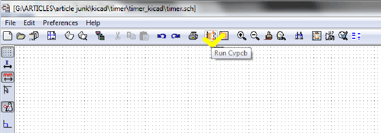
Now run cvpcb by to convert the components into modules that we can use while designing the circuit board:
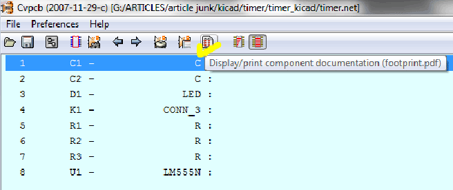
The cvpcb window will look like this:

For each component listed we must select the required area. It would be better if you listed the entire occupied area without filtering:

How can I identify which footprint will be appropriate for a specific component?
Any footprint you select must match the physical dimensions of the components in your collection. You can view the entire available footprint in pdf format using the button shown below:
In your PDF viewer, set the zoom to 100% or full size. Now just place the component gently on the screen, just above the footprints of the specific component and see if it matches or not. Note the label for that space and simply select the space with the same label from the list for that specific component.

I have some small electrolytic capacitors for the circuit that match the following footprint, like:

If you want to see the selected footprint in detail, keep the selected footprint in the list and press view selected part:

Here is the footprint in detail:
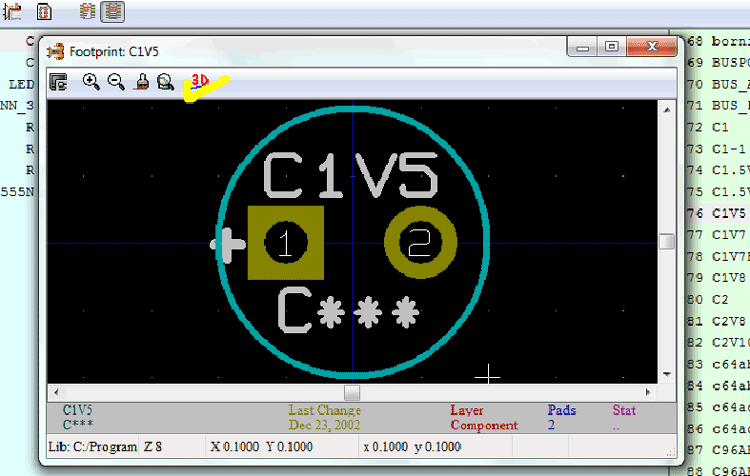
If you want to see the component in 3D, you can press the 3D button.
3D view of the component:

Close both windows and double-click on the required area to select it. If you finish selecting the footprints, the page will look like this:

Save the netlist using the save button:

Now run the pcb editor using the “Run Pcbnew” button in the schematic editor or main window.

PCB Editing
3) PCB Editing
Here is the PCBNEW window:

Before we proceed, I recommend that you make the necessary page settings, as we did for the schematic editor. After that, it would be best to draw up an initial sketch of the framework, which we can change later if necessary.
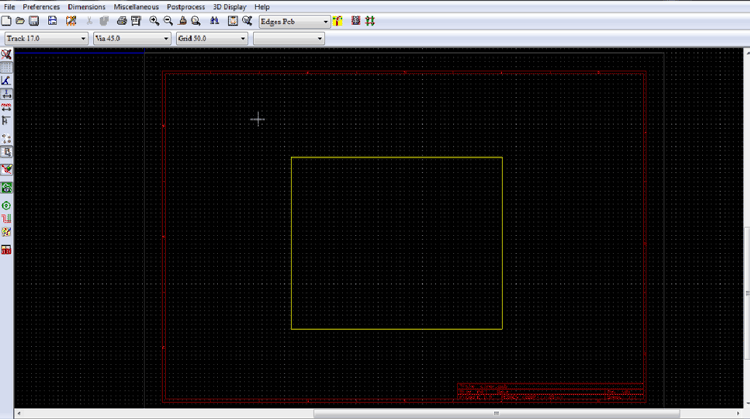
Select the current working layer as “Edges Pcb”.

Use the graphic line button to draw the borders. You can set the coordinates at any corner to zero by holding the mouse pointer over it and pressing the spacebar. Double click to finalize the outline as you finish drawing it.
Here I have drawn a square outline for the PCB.
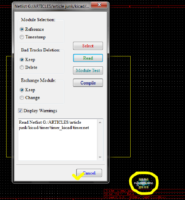
Now let's link the schematic and the pcb editor by reading the netlist.

Press the “read” button for the next window.

In the following figure you can see that the modules corresponding to the components of the schematics have been added to the pcb editor. Now press the cancel button.
Now arrange the components by moving them to the appropriate positions and orientations. Use M to select a component to move with the cursor.
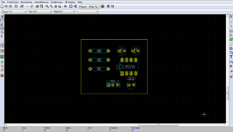
After rearranging the components:

Now it appears that the board outline is too large for the circuit. Now I'm going to show you how to delete items, in this case we are only deleting the outline.
Drag the cursor across the block by keeping the left button pressed and release so that the entire block is selected. Now right click and select the delete block option.

For this specific case, select “include border layer” and press OK.

You can use the same technique to delete tracks, modules, zones, texts, drawings, etc.
After deleting the current outline, we will draw a much smaller one. After rearranging the components and redrawing the outline, the PCB editor will look like this.
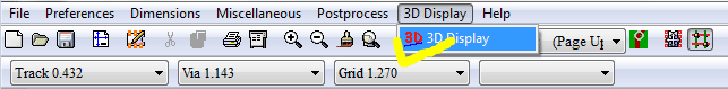
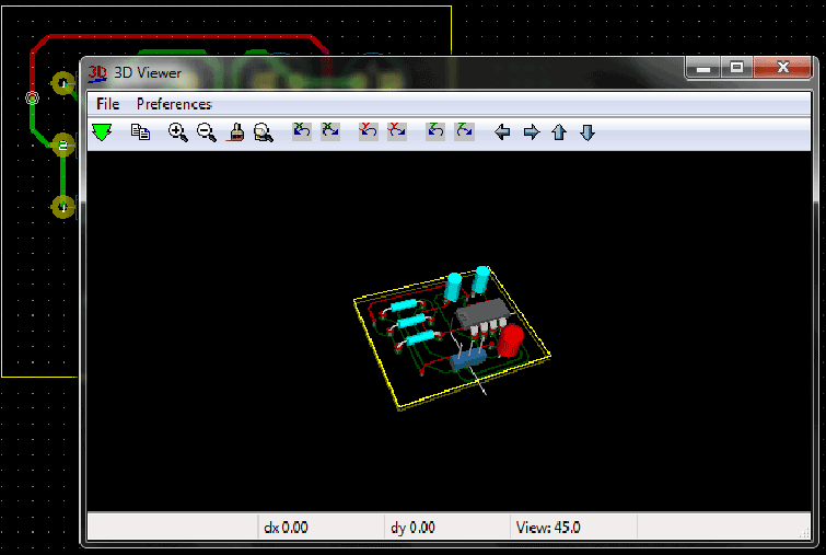
At this point you must make sure that the arrangement of the components on the board is physically feasible. Otherwise, you will have a lot of problems assembling the components. To avoid such problems, there is the option to view your board in 3D. Click the 3D view button.
If you are happy with the arrangement of the components on your board, you can begin routing.
Before that you have to define some things. Go to general options where you can set the number of layers required, maximum links shown, etc.

I'm going to make a 2-layer board, which isn't actually necessary for this simple circuit, but I can show you how to add vias and tracks on both layers.
Press the OK button to save the settings:

Now we will mainly work on the two important layers of our board
1) Copper layer – normal lower layer if we consider a single layer board, where we do the soldering.
two) Component Layer – The opposite side of the board where we place the components.
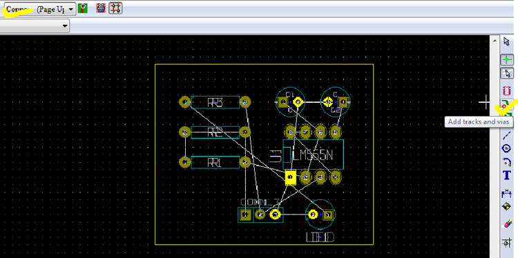
Now the PCB editor window will look like this.

You can click any pin to highlight corresponding connected pins after clicking the “Network Highlight” button as shown above.
In the following pins, a set of highlighted pins are shown. You can now add tracks by connecting these pins using the “Add Tracks and Vias” tool. Make sure you have selected “Copper (page above)” from the drop-down list as marked in the figure.
Now you can place the track by connecting the pins. Use the END key to release the track when you reach the end point.
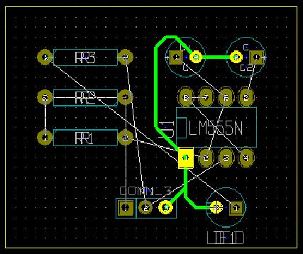
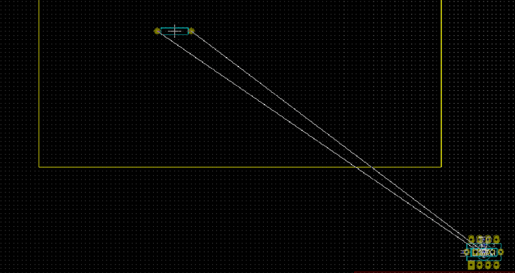
In the following figure it is shown that I am having problems connecting pin 7 and the pins of two resistors R2 and R1.
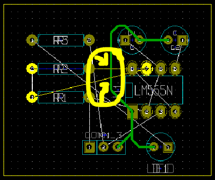
Then I will place a part of the track on the component layer and connect the rest to the copper layer via vias.
First connect both ends of the resistors normally. Now start adding the track from pin 7, and when you get to the point where you want to add the via, right click and select “place Via” or just press V.

Now you can simply route through the component layer and connect both parts via another via, as shown in the following figure.
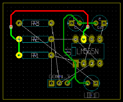
Remember that your component's pin can also act as a via, as it is printed through the hole (PTH), connecting the two layers.
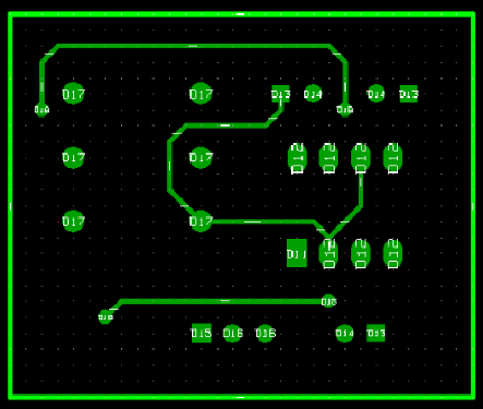
I have completed the routing and my design is shown below.
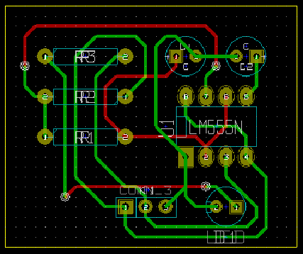
Now let's have a 3D view of our board.
Generating Gerber file
4) Generating Gerber file
Select the chart after clicking the file to open the chart window.

Do things in the plot window as shown in the following figure:

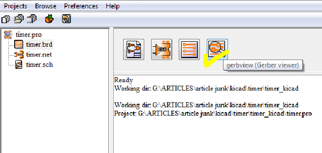
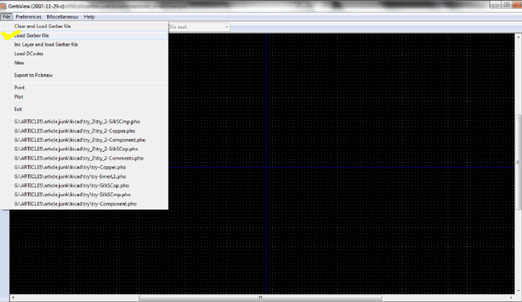
Now go to the main window and click on the “gerbview” button to open the Gerber viewer.
The following figure shows the Gerview window. Select “Upload Gerber file”
Let's look at the copper layer first.
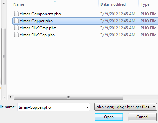
Gerber visualization for the copper layer:

To view another file without mixing the view with the previous one, use the “Clear and load gerber file” option.

This time we select the component layer:
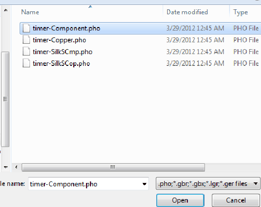
The Gerber view of the component layer will look like this:
To view all layers at once, use the “Inc Layer and Load gerber file” option.

The Gerber view of the selected layers will look like this:

Now you select the “Save configuration” option.

Save the gerview file with the .cnf extension

Now click on the save button and we are done. The next step is to send the Gerber files to your PCB manufacturer. All the files you have to send depend on the printed circuit board manufacturing process they have.