There are 2 cutoff frequencies for band-reject filter.
1. upper cutoff frequency (f1) – the frequency below which all frequencies are passed
2. lower cutoff frequency (f2) – all frequencies above this frequency are passed
Similar to bandpass filter, but the difference is f1
1. Broadband Reject Filter – Suppresses a wide range of frequencies.

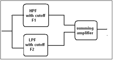
Fig. 1: Broadband Reject Filter Overview
2. Narrowband pass filter – suppresses single frequency or few frequencies close to the central frequency.
Broadband Reject Filter
It is actually a combination of LPF and HPF as shown in the figure
Here F1 > F2. So we have to design HPF with F1 and LPF with F2. Suppose we want to suppress the frequency band between 10 KHz and 20 KHz. so F1 = 20,000 Hz and F1 = 10,000 Hz.
Designing HPF section
Step 1: Assume the required value of the capacitor. must be less than 0.1 micro Farad. This is necessary for better frequency stability. Suppose we assume the C value as 1 nF (nano farad)

Fig. 2: Screenshot of the calculations required to find the passband resistance and gain for the HPF section
Designing LPF section
Step 4: Assume the required value of the capacitor. Suppose we assume the value C as 10 nF

Fig. 3: Screenshot of the calculations required to find the passband resistance and gain for the LPF section
The final project with component values are shown. The operational amplifier is an active component and requires +ve and -ve bias voltages. You can test the circuit by applying the input through the signal generator and observing the output on the DSO or oscilloscope, as well as on the goat plotter, as shown in the figure.

Fig. 4: Circuit diagram of IC LM741 OPAMP based band-rejection filter
Note: – Schematic design is prepared in NI multisim 11 software. The software is available free of charge for a 1-month trial period on the NI website.
Narrow bank rejection filter (Notch filter)
Step 1: Select the notch frequency which is the frequency to be rejected. Mainly these filters are used to remove the power line frequency of 50 Hz. So consider Fn = 50 Hz
Step 2: Assume the value of capacitor C as 1 micro F (because the frequency is very low, the value of the capacitor must be large)

Fig. 5: Screenshot of the calculations needed to find the resistance of the Notch Filter
Step 5: To construct a T-network with C – R/2 – C, we need the value R/2. Then connect two resistors in parallel with the same value R
Step 6: To construct a T-network with R – 2C – R, we need the value 2C. Then connect two capacitors in parallel of the same value C
The final design is shown below.

Fig. 6: Circuit diagram of Notch filter based on IC LM741 OPAMP
Circuit diagrams
| Circuit Diagram-LM741-OPAMP-IC-Based-Notch-Filter |  |