There are 2 cutoff frequencies for bandpass filter.
1. upper cutoff frequency (f1) – the frequency below which all frequencies are passed
2. lower cutoff frequency (f2) – all frequencies above this frequency are passed
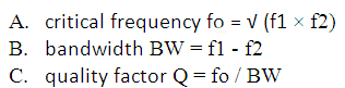
From these f1 and f2 we will define the following parameters which are designing parameters for bandpass filter.

Fig.1: Screenshot listing different parameters for bandpass filter
Based on Q we have two types of bandpass filter
1. Broadband pass filter – with Q <10 it has a wide flat response across the entire frequency range. BW is more
2. Narrowband pass filter – with Q>10 it has a clear bell-like response. BW is much smaller.
Broadband pass filter
It is actually a combination of LPF and HPF as shown in the figure

Fig. 2: Broadband pass filter overview
Here F2 > F1. So we have to design HPF with F1 and LPF with F2. Suppose we want to pass the frequency band between 2 KHz to 5 KHz. so F1 = 5000 Hz and F2 = 2000 Hz.
Designing HPF section
Step 1: Assume the required value of the capacitor. It must be less than 0.1 micro Farad. This is necessary for better frequency stability. Suppose we assume the C value as 10 nF (nano farad)
Step 2: calculate the resistance value from the equation

Fig. 3: Screenshot of the calculations required to find the HPF resistance in the broadband pass filter

Figure 4:
therefore, our assumption for the capacitance value as 10 nF is good (or OK). Otherwise, if the calculated value of R is much less than 1 KOhm, we will have to assume some other value of the capacitor. Because the R value should not be less than 1 K Ohm.
Step 3: Choose the required passband gain. Suppose we take this as 2. Then form the equation
Af = 1 + (R2/R1)
2 = 1 + (R2/R1)
R2/R1 = 1
R2 = R1

Figure 5: Screenshot of the calculations required to find the HPF resistance in the broadband pass filter
Designing LPF section
Step 4: Assume the required value of the capacitor. Suppose we assume the same value C as 10 nF
Step 5: Calculate the resistance value from the equation

Figure 6: Screenshot of the calculations needed to find the LPF resistance in the broadband pass filter
This value is an odd value of the resistor. May not be available as a fixed amount. So can we use 4.7K potentiometer? and adjust it to the desired value.
Step 6: Choose the required passband gain. If we consider this as 2, then again
R2 = R1

Fig. 7: Screenshot of the calculations needed to find the LPF resistance in the broadband pass filter
The final project with component values are shown. The operational amplifier is an active component and requires +ve and -ve bias voltages. You can test the circuit by applying the input through the signal generator and observing the output on the DSO or oscilloscope, as well as on the goat plotter, as shown in the figure.

Fig. 8: Circuit diagram of wideband pass filter based on IC LM741 OPAMP
Note: – The schematic design is prepared in NI multisim 11 software. The software is available free of charge for a 1-month trial period on the NI website. Next, all circuits are also prepared in the multisim 11 software.
Narrowband pass filter
Step 1: For simplicity, assume C1 = C2 = C
Step 2: select center frequency fc = 2 KHz, passband gain Af = 2 and Q = 10
Step 3: Assume the value of capacitor C as 100nF
Step 4: calculate the R1 value of

Fig. 9: Screenshot of the calculations needed to find the resistance of the narrow bandpass filter
The final design is shown below.

Fig. 10: Circuit diagram of narrowband pass filter based on IC LM741 OPAMP