In previous tutorials, amplifier circuits were designed to amplify single-channel audio. The last decade has seen a boom in audiophile. This brought a revolution in the music industry. Now, people like to listen to high-resolution surround music like a 3D video. A surround sound system is designed to create a sound field as if the sound is coming from the back, front, left and right sides. It can also create sound above the listener. Surround sound system is used in cinemas and theaters to give a realistic feeling to the audience. An alternative to the surround sound system is the stereo audio system. There are basically two sound systems –
1) Mono Sound System – The mono system produces a natural mono sound that comes from a single channel and is reproduced by a single speaker. Although more speakers can be added to play the same audio channel, a copy of the same sound will be played on all speakers in that system.
2) Stereo Sound System – In the stereo sound system, stereophonic sound, also known as stereo sound, can be heard through different channels using more than one speaker. Generally by stereo system it is understood that there are two independent audio channels that are reproduced by two or more speakers separately. This system is widely used in headphones. To design a stereo sound system, you need two channels as well as the audio source that can provide the stereo sound. So that the audio signal of two audio channels can be obtained and the sound can be played on different speakers.
For a stereo sound system, the same number of amplifiers is required as the number of audio channels. In this tutorial, a stereo power audio amplifier will be designed using IC TDA2822. TDA2822 is a dual power amplifier with two independent amplifier circuits on the same chip. The IC can be used as a bridge or stereo audio amplifier. In the circuit designed in this tutorial, the IC is used as a stereo power amplifier to boost the audio channels and send audio to two separate speakers.
In the introductory article of this series, various design parameters of audio amplifier circuits were discussed such as gain, volume, slope rate, linearity, bandwidth, clipping effect, stability, efficiency, SNR, output power, THD and grounding. loop. This amplifier circuit will be designed considering the following design parameters –
Gain (voltage) – 39 dB
Bandwidth – 20 Hz to 20 KHz
Output power – 1 Watt
The amplifier will be designed to deliver audio to two speakers with an impedance of 8 ohms. The circuit will have the following additional features –
– No clipping effect
– Stereo output
Circuit design will be followed by circuit testing to verify the intended design factors.
Required components –
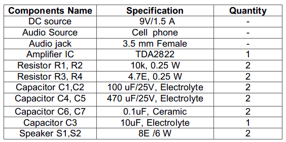
Fig. 1: List of components required for TDA2822H IC-based stereo audio amplifier
Block diagram –
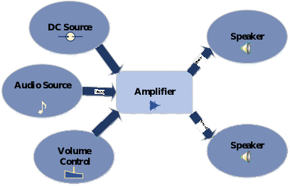
Fig. 2: Block diagram of TDA2822 IC based stereo audio power amplifier
Circuit Connections –
The amplifier circuit is constructed by assembling the following components –
1) DC Source – The amplifier circuit is powered by a 9 V, 1.5 A battery. The power supply is passed through a capacitor (shown as C3 in the circuit diagram) of 10 uF . This is a filtering capacitor to remove any unwanted ripples from the power supply.
2) Audio Source – Audio input is provided by a smartphone. To receive audio from the smartphone, a 3.5 mm audio jack is connected to the phone. The 3.5mm audio jack has three wires – one for ground and two wires for the left and right channels. Since the amplifier is designed for both channels, both channel wires will be connected to the amplifier as audio input. Both channels are used to apply stereo sound to the amplifier input. The connector's ground wire will be connected to the circuit's common ground. Generally, the audio signals on these two channels are 180 degrees out of phase, making the system a balanced audio system.
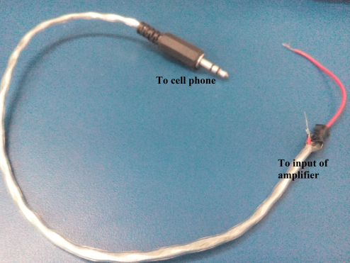
Fig. 3: Typical 3.5mm audio jack image
3) TDA2822 Dual Power Amplifier – TDA2822 is a dual power amplifier IC. This IC can operate over a wide range of supply voltages ranging from 3V to 15V. There are two independent operational amplifiers in the IC. This IC is specially designed for use in portable radios and transistor arrays. It is well known for its low crossover distortion and low quiescent current.
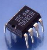
Figure 4: Typical image of TDA2822 dual power amplifier IC
The TDA2822 has the following pin configuration –
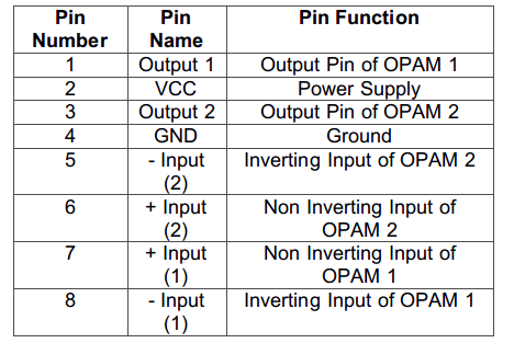
Fig. 5: Table listing the pin configuration of the TDA2822 dual power amplifier IC
The IC has the following pin diagram –
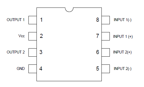
Fig. 6: Pin diagram of TDA2822 dual power amplifier IC
The IC has the following functional diagram –
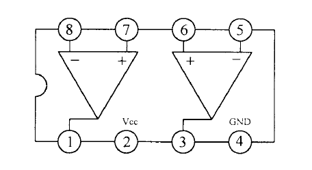
Fig. 7: Functional Diagram of TDA2822 Dual Power Amplifier IC
The TDA2822 is used as a stereo power amplifier in the circuit. The IC can provide a closed loop gain of 39 dB which is equivalent to a voltage gain of 90. The voltage gain of this dual amplifier IC is not adjustable as it is internally restricted to just 39 dB.
The left audio channel of the audio connector is connected to the non-inverting input of OPAM 1, while the right audio channel of the audio connector is connected to the non-inverting input of OPAM 2. The inverting input pins 8 and 5 of OPAM 1 and 2 are respectively connected to ground through a filter capacitor (shown as C1 and C2 in the circuit diagram, respectively) of 100 uF . These capacitors are connected for ripple rejection. The output of OPAM 1 is taken from pin 1 of the IC which is connected to one of the speakers, while the output of OPAM 2 is taken from pin 3 of the IC which is connected to another speaker. At the output pin, capacitors (shown as C4 and C5 in the circuit diagram) of 470 uF are connected to block the passage of any DC components from the amplifier to the output load. Any DC component from the amplifier to the load which is the speaker in this case can damage it or produce noise or distortion in the output audio. There is an RC circuit (shown as C6 and R3 in the circuit diagram) connected to the output pin of OPAM 1 and an RC circuit (shown as C7 and R4 in the circuit diagram) connected to the output pin of OPAM 4. Both of these RC circuits are made up of a 0.1 uF capacitor and a 4.7 ohm resistor. These RC circuits help to stabilize the output frequency.
It should be noted that in this circuit TDA2822H is used as TDA2822 IC. There are also other TDA2822 models available that have different configurations and pin diagrams.
4) Speakers – There are two speakers of 10 Watt Power rating and 8 ohm Impedance used as load on the output of the operational amplifiers. The speakers are connected to pins 1 and 3 of the IC, which are the output pins of the TDA2822, and the speaker ground wires are connected to the common ground. 10 Watt rather than 6 Watt speakers are used as per availability.
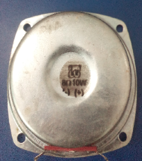
Fig. 8: Typical image of a 10 W, 8 Ohm speaker
The following precautions should be taken while assembling the circuit –
1. Always use the filtering capacitor on the power supply input terminal to avoid unwanted ripple.
2. Use the equivalent or high power speaker as the amplifier output power.
3. Always use a capacitor in series across the amplifier output to block any DC components.
4. Always calculate the maximum power of the amplifier before connecting it to the speaker. The practical value may differ from the theoretical one.
5. Avoid clipping the output signal, as this may damage the speaker.
6. Always place components as close together as possible to reduce noise in the circuit.
7. Always follow star topology when grounding, this will keep the noise low and reduce the loop grounding problem.
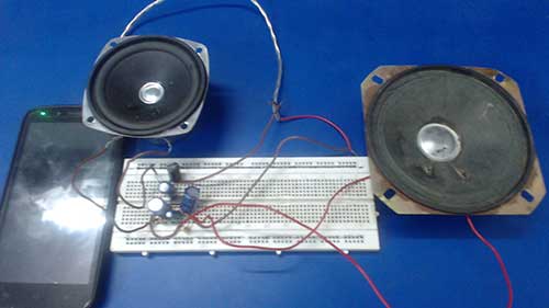
Fig. 9: Prototype of stereo audio power amplifier based on IC TDA2822
How the circuit works –
To generate stereo sound from two speakers, IC TDA2822 is used. The IC is designed to be used as a stereo amplifier or bridge amplifier. Internally it consists of two operational amplifiers. To make a stereo amplifier, the circuit connections are made as indicated in the TDA2822 technical sheet. The IC can provide a wide range of output power according to the input supply voltage and output load. The output power of the IC’s integrated op amps has been summarized in the following table –
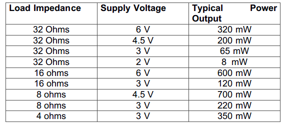
Fig. 10: Table listing the power output of the integrated operational amplifiers of the TDA2822 IC
The output power specified in the table above is tested for a frequency of 1 KHz as per the data sheet. Since the speakers used in the output have an impedance of 8 ohms and a supply voltage of 9 V is supplied to the IC, the typical output power of OPAM should be 1 Watt. The voltage gain is internally adjusted to 39 dB or 90, which cannot be changed.
The maximum input voltage limit for the IC is fixed so that the output power limit cannot be exceeded. When exceeding the output power above 1 Watt, the output signal will begin to clip. This will add distortion and noise to the output audio. The root mean square (RMS) voltage at the output can be calculated by the following equation –
Po = (Vrms)2/R
where,
output power, Po = 1 Watt
Load resistance, R = 8 ohms
Therefore, the RMS (root mean square) voltage, Vrms is as follows –
1 = (Vrms)2/8
Vrms = 2.8V
The audio signal is a sine wave, so its peak-to-peak voltage for 1 Watt power can be calculated as follows –
Vp-p = Vrms*(2)1/2
Vp-p = 2.8*1.414
Vp-p(maximum)= 4 V (approx.)
As the voltage gain of the IC is fixed at 90 or 39 dB, the maximum input voltage can be calculated as follows –
Gain = V(pp)output/Vin(pp)
Vin(pp) = 4/90
Vin(pp) = 45 mV (approx.)
Therefore, the maximum amplitude (voltage level) in the input audio signals should not be more than 45 mV, otherwise the output signal will begin to clip.
Testing the circuit –
For testing the amplifier circuit, the function generator is used as the input source. The function generator is used to generate a sine wave of constant amplitude and frequency. Any audio signal is also basically a sine wave, so a function generator can be used instead of a microphone or actual audio source. Thus, the function generator can be used as an input source to test the audio amplifier circuit. During testing, also at the output, a speaker is not used as a load, as the speaker is resistive as well as inductive. At different frequencies, its inductance changes, which in turn changes the impedance (R and L combination) of the speaker. Therefore, using a speaker as a load on the amplifier output to derive its specifications may generate false or non-standard results. In place of the speaker, a purely resistive dummy load is used. Since the resistance does not change with frequency, it can be considered a reliable load regardless of the frequency of the input audio signal.
To test the amplifier circuit, first the input voltage is set within the applicable range of up to 45 mV. The frequency of the input signal is set to 1 KHz. Then, the output waveform is observed in CRO and the input signal is boosted until the output waveform begins to clip.
With dummy load of 10 ohm impedance, the following observations were noted –

Fig. 11: Table listing the output characteristics of the TDA2822 IC-based stereo audio power amplifier
Ideally, the amplifier output power should be 1 watt. As the load impedance is now 10 ohms, the following output power of the amplifiers must be obtained –
Po = V2(pp)/2R
Po = (4*4)/(2*10)
Po = 800mW
Therefore, practically the output power of this stereo amplifier for the actual speaker load varies between 800 mW to 1 watt. From the output waveforms, it was observed that when keeping the input voltage level below 45 mV there was no clipping effect.
The stereo power amplifier designed in this tutorial can be used in portable cassette players. The circuit can also be used as a headphone amplifier for headphones with an impedance of 4 ohms to 32 ohms. In the next tutorial, a preamplifier using IC MAX4468 will be designed.

