In one of the previous tutorials, an SMPS closed-loop boost converter with fixed output voltage was designed. In this series, the following SMPS circuits are designed –
1. Boost Converters –
a) Open loop boost converter
b) Closed-loop boost converter
c) Open Loop Boost Converter with adjustable output
d) Closed Loop Boost Converter with Adjustable Output
2. Buck Converters –
a) Open Loop Buck Converter
b) Closed-loop Buck Converter
c) Open Loop Buck Converter with Adjustable Output
d) Closed-loop buck converter with adjustable output
3. Buck-Boost Converters
a) Buck Open Loop Inverter – Boost Converter
b) Buck Open Loop Inverter – Boost Converter with Adjustable Output
4. Flyback Converter
5. Push-pull converter
The closed-loop boost converter designed in the previous tutorial had a constant, regulated voltage at the output, but it could not be varied. For stable output, the Boost converter had an error detection circuit. Error detection was done by adding a feedback circuit that continuously checks the error in the output voltage and provides a regulated voltage at the output. To make the output of the circuit adjustable, it must be passed through a variable resistor. This closed-loop boost converter not only had a feedback circuit, but its output was also adjustable.
Therefore, in this tutorial, a closed-loop non-isolated boost converter is designed. The boost converter can be designed in two ways-
Open Loop Boost Converter – In open loop boost converter, there is no feedback from the output to the input, unlike the closed loop which has a feedback circuit. Therefore, the output of an open-loop boost converter is not regulated.
Closed-loop boost converter – In closed-loop boost converter, there is feedback from the output to the input. Therefore, the output of a closed-loop boost converter is regulated.
There are certain design parameters involved in the design of the boost converter. It is important to understand these design parameters. Any boost converter can operate in any of the two possible operating modes. These modes of operation are as follows –
• Continuous Conduction Mode (CCM)- In CCM, the current in the inductor is continuous throughout the entire switching period cycle. Thus, a regulated voltage at the output is obtained, but the output is regulated only if the current is drawn within the limits of the CCM.
• Discontinuous conduction mode (DCM)- In this mode, the current in the inductor is pulsating and becomes zero during a part of the switching time. Therefore, a regulated voltage is not received at the DCM. However, the voltage can be regulated by connecting a feedback circuit from the output to the input.
In this tutorial, a non-isolated boost converter is designed, which means the input and output share the same ground. The boost converter designed in this project will have an output voltage ranging from 5V DC to 9V DC with a tolerance limit of +/-0.5V. Once the circuit has been designed and assembled, the value of the output voltage and current will be observed using a multimeter. These values will indicate the efficiency of the boost converter designed in the project.
Required components
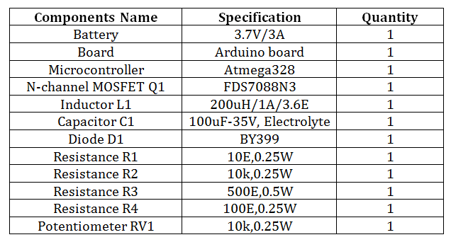
Fig. 1: List of components required for the Adjustable Closed Loop Boost Converter
Block diagram –
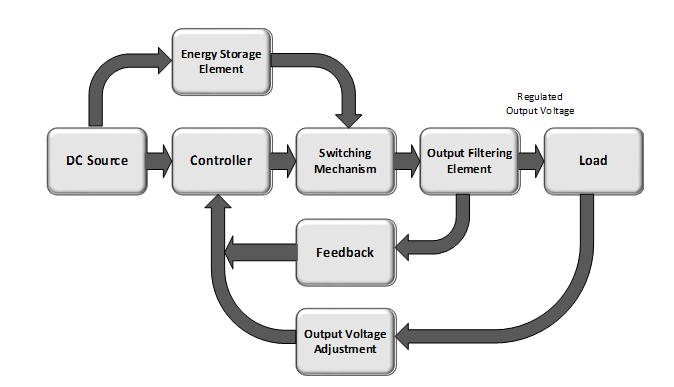
Fig. 2: Block diagram of adjustable closed-loop boost converter
Circuit Connections –
In this project, a closed-loop boost converter operating in DCM mode is designed and component values as per standard DCM equations are calculated for the desired output.
The boost converter designed in this tutorial will have the following design parameters –
Input voltage, Vin – A 3.7V Li-ion battery will be used as the source. The battery voltage will be the input voltage.
Output voltage range , Vout – The output voltage will be adjustable between 5V and 9V.
Maximum output current, Iout (max) – The maximum output current limit will be 100 mA. The critical output current limit will be 10mA.
Output ripple voltage ( dV ) – The maximum output voltage ripple assumed at the output will be 100mV.
Load resistance – In this circuit, a resistance will be connected to the output that will act as a load for the circuit. The maximum resistance value can be calculated using Ohm’s law, which is as follows –
For Vout = 9V
Vout = Iout(max)*RL
RL(max) = Vout/Iout(max)
Putting all the values,
RL = 90E
Now the nominal power of the resistance can be calculated as follows – P = (Vout)2/(RL)
Putting all the values,
Pout = 0.9W
For Vout = 5V
Vout = Iout(max)*RL
RL(max) = Vout/Iout(max)
Putting all the values,
RL = 50E
Now the nominal power of the resistance can be calculated as follows – P = (Vout)2/(RL)
Putting all the values,
Pout = 0.5W
Therefore, a variable resistor with the available resistance range as calculated above will be used as a load on the output for maximum efficiency.
Frequency (Fs) – The frequency of the PWM signal generated by the microcontroller should not be too high or low, therefore a frequency of 10 KHz is selected to operate the switching components of the circuit. The frequency value is assumed.
The boost converter has the following circuit blocks –
1. DC Source –
A 3.7V lithium-ion battery is used as the input power source in the circuit. The battery voltage itself is the input voltage to the circuit.
2. Controller and switching mechanism –
An oscillator is used to generate a pulse width modulated (PWM) signal of a desired frequency. In this boost converter, Arduino UNO is used to generate the PWM signal, so the Arduino board acts as an oscillator. The PWM signal is a pulse train used to turn the MOSFET on and off. MOSFET is used as switching transistor in the circuit.
For switching purposes, a transistor and a diode are used as switching components. For transistor selection, MOSFET is chosen as FETs are known for their fast switching speed and low RDS (ON) (drain to source resistance in ON state). Therefore, an N-channel FDS7088N3 MOSFET (shown as Q1 in the circuit diagram) is connected in parallel to the input DC source which acts as a switch in the circuit as its threshold voltage is very low, around 2V. Therefore, it can be easily powered by a 3.7V battery. In the ON state, the Vds of the FDS7088N3 MOSFET is also very low, which reduces the power dissipation of our circuit.
To turn the MOSFET on and off, a pulse train must be applied to its gate. To do this, the controller board generates a 10kHz pulse width modulated signal. This PWM signal is used to turn the MOSFET on and off. To generate the controller's PWM signal, an Arduino sketch was written to the board. This Arduino sketch can be downloaded from the code section.
It should be noted that the switching time of the MOSFET and diode must be less than the rise and fall time of the PWM wave. A gate-to-source resistance must be used to prevent any unwanted triggering of the MOSFET by external noise. It also helps to quickly turn off the MOSFET by discharging its parasitic capacitance.
A low resistor value (10E to 500E) must be connected to the gate of the MOSFET. This will solve the ringing (eddy oscillations) and spike current problem in the MOSFET. The PWM signal voltage level must be greater than the MOSFET threshold voltage. So that the MOSFET can be turned ON completely with minimum RDS (ON). There must be a heat sink mounted with the MOSFET to dissipate excess heat, otherwise the FET may be damaged.
Another switching component used in the circuit is a diode. The diode switching time must be less than the rise and fall time of the PWM wave. The Arduino board generates a PWM wave with a rise time of 110ns and a fall time of 90ns. The forward voltage drop of the diode must also be very low, otherwise it will dissipate power, which will further reduce the efficiency of the circuit. The diode must offer low voltage drop in forward bias and the RDS (ON) of the MOSFET must be low. Therefore, in this experiment, a BY399 diode that best suits the circuit design is selected.
Before generating the PWM signal, the switching frequency of the circuit needs to be decided. For this boost converter, a switching frequency of 10kHz is selected, which will work well in this converter design.
The duty cycle of the generated PWM signal is another important consideration as it will decide the active state of the MOSFET. The duty cycle can be calculated as follows –
D% = 1- (Vin/Vo)*100
Vo=Desired output voltage, 5V to 9V
Vin = Input voltage, 3.5 V
Since the output voltage varies from 5V to 9V, the duty cycle will be calculated for both 5V and 9V.
For Vo(min) = 5V
D(min)% = (1-(3.5/5))*100
D(min)% = 30% (approx.)
For Vo(max) = 9V
D(max)% = (1-(3.5/12))*100
D(max.)% = 60% (approx.)
A capacitor and resistor of appropriate value should be used to generate the frequency of 10 kHz and the duty cycle of 30% to 60%. The higher the frequency selected for the switching components, the greater the switching losses. This decreases the efficiency of the SMPS. But the high switching frequency reduces the size of the energy storage element and improves the transient response of the output.
3. Energy storage element –
An inductor is used to store electrical energy in the form of a magnetic field. Therefore, the inductor acts as an energy storage element. An inductor of value 200 uH is used in the circuit. For an inductor, a secondary or primary coil of a transformer, a relay coil, or any standard inductor that has the desired inductance value can be used.
4. Output filtering element –
As a filtering element, a capacitor (shown as C1 in the circuit diagram) is used at the output of the circuit. In normal operation of the Boost circuit, transistor Q1 turns on and off according to the frequency of the oscillator circuit. This generates a pulse train in inductor L1 and capacitor C1, as well as transistor Q1. Since the capacitor is connected to the inductor only in the negative cycle of the PWM signal, this forms an LC filter that filters the pulse train to produce a smooth DC at the output. The value of the capacitor can be calculated using the following DCM equation –
Capacitor C >= (Io(max) * (1- (2*L1*Fs/RL(max))1/2))/ (Fs*dV)
For RL = 90E, putting all values in the above equation,
C1 >= (0.1*(1-(2*200*10-6*10,000/90) 1/2))/ (10,000*0.1)
C1 >= 78uF
As the capacitor can be larger than the calculated value, any capacitor with a value equivalent to 78uF or greater than 78uF can be used.
As it is the minimum value of capacitor required, so in the circuit a standard value capacitor is used which can be easily available, hence a capacitor of 100 uF is used.
5. Feedback loop –
In the previous tutorial, it was seen that without any feedback circuit, a high voltage was received at the output when there was no load connected. When any load on the output was connected, the output voltage dropped below the desired output voltage. therefore, there was a need to regulate the output voltage by connecting a feedback circuit.
Therefore, in this circuit, feedback is provided from the output terminal to the input terminal which regulates the output voltage even when there is no load present at the output. The Feedback circuit must calculate the voltage error and then the microcontroller automatically adjusts the output voltage according to the desired voltage. This error voltage adjustment is managed by the Arduino sketch running on the board.
To provide feedback, a ladder of resistors is used at the output (as shown in the circuit diagram). To calculate the value of the resistor network, the maximum output voltage of the open loop circuit must be known when no load is connected to the output. This will be the desired output voltage that should feed from the resistor divider network to the analog pin of the controller (as shown in the circuit diagram). The output voltage must be equal to 5.2 V as the microcontroller provides 5.2 V as a reference voltage. The value of the resistor network can be calculated as follows-

Fig. 3: Circuit diagram of the resistive ladder used as feedback in the closed-loop boost converter
According to the resistor divider rule –
Vr = Vo*(R4/R3+R4)
Where,
Vr = desired output for analog pin
Vo = output voltage of the open-loop boost converter without load.
It was observed that the values of Vr and Vo are –
Vo = 20V
As the potentiometer is powered by a 3.3V source, then Vr= 3.3V. This will match the feedback scale with the potentiometer.
Assuming R3 = 500And now R4 is –
3.3 = 20*(R4/500+R4)
R4 = 100E (approx.)
So R3 = 500E and R4 = 100E
Now, the rated power of resistor R3 and R4 can be calculated as follows –
(For R3),P3 = (Vo-Vr)2/(R3)
Putting all the values,
P3 = 0.5W (approx.)
(For R4), P4 = (Vr)2/(R4)
Putting all the values,
P4 = 0.1 (approx.)
6. Output voltage adjustment –
To vary the output voltage, a potentiometer is used at the output of the circuit (as shown in the circuit diagram). The potentiometer is powered by the battery and then the analog pin of the microcontroller senses the voltage of the potentiometer. After detecting the voltage, the microcontroller adjusts the duty cycle according to the desired output voltage. Thus, by turning the potentiometer knob, the output voltage can be varied as needed.
How the circuit works –
Any SMPS has some switching components that turn on and off at high frequency and has some storage component that stores the electrical energy while the switching components are in conducting state and discharges the stored energy to the output device while the switching components are not driving. state.
A simple boost converter consists of the inductor (L), a diode (D), a capacitor (C) and a transistor where the transistor acts as a switch. In the boost circuit, when the switch is closed, i.e., the switching component is in a conducting state, the inductor starts generating a magnetic field and stores energy. The energy stored in the inductor increases the output voltage compared to the input voltage.
When current begins to flow through the switching component, as its path is less resistive compared to the parallel path containing the capacitor and output load, the inductor generates a positive polarity at its left terminal and negative at its right terminal. . Due to the change in polarity, the diode becomes reverse biased. In this condition, the capacitor, which was charged in the previous cycle, supplies current to the load while the switching component goes into a non-conducting state or opens between ground.
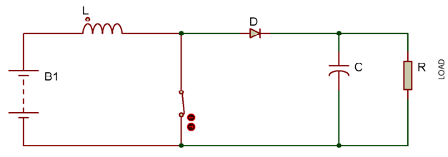
Fig. 4: Circuit diagram showing the ON state of the switching component in the Boost converter
When the switch is open, the current is reduced as the impedance increases, so the magnetic field generated in the inductor begins to collapse and the polarity of the inductor reverses. This makes the diode forward biased and the capacitor now starts charging with a voltage higher than the input voltage. Since the input now has two sources in series, one is the inductor and the other is the battery. Therefore, the output voltage is always greater than the input voltage.
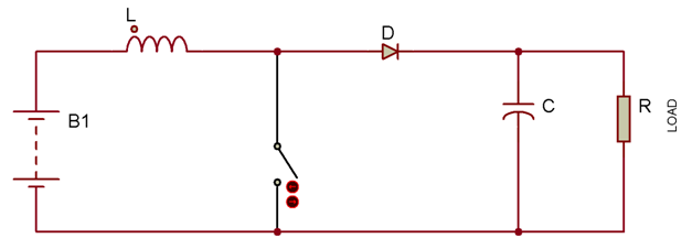
Fig. 5: Circuit diagram showing the OFF state of the switching component in the Boost converter
Therefore, in the ON state, the Diode was in Blocking Mode (OFF) and the Transistor was ON. In the OFF state, the Diode was in conduction mode (ON) and the Transistor was OFF.
So, it can be said that the Boost Converter has two switching components – one is the transistor and the other is the diode. At a time, only one of the switching components conducts, that is, it is in the ON state, while the other enters the non-conducting state, that is, it enters the OFF state.
This is how any boost converter works. The boost converter designed in this project is closed i.e. a feedback circuit is added to it. Feedback is provided through a voltage divider network. The output voltage is detected by the voltage divider resistor ladder and supplied to one of the pins of the microcontroller. The microcontroller board used in the project is Arduino. The Arduino's built-in ADC channel converts the detected voltage into a digitized reading.
The Arduino is programmed to compare the output voltage with a reference voltage and the difference between the two is the error voltage. To compensate for the voltage error, the Arduino is programmed to change the duty cycle of the PWM signal that controls the transistor circuit. By changing the duty cycle of the PWM signal, the output voltage is modified to the desired output. Due to the presence of a variable resistor at the output, the output voltage can vary within the desired range.
Testing the circuit –
In this circuit, a variable resistor is added to the closed-loop boost converter circuit to make the output voltage adjustable. The Arduino sketch is also modified to change the duty cycle of the PWM signal according to the variable resistor voltage input.
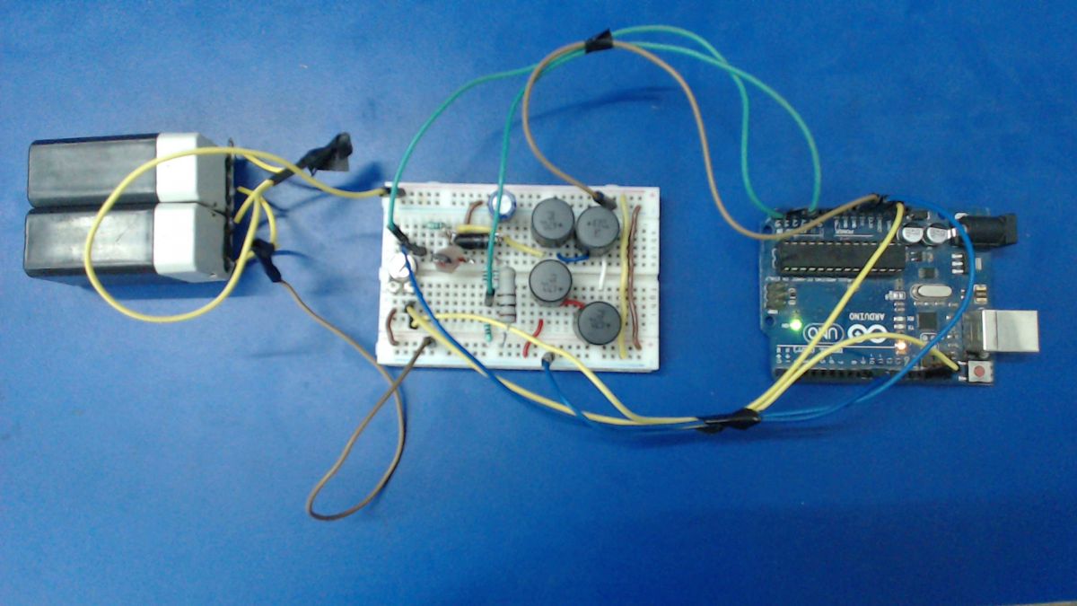
Fig. 6: Closed-loop boost converter prototype designed on a breadboard
In the circuit, Battery Voltage, Vbat/Vin = 3.7V
While measuring voltage and current values with different loads at the output when the duty cycle is set to 60 percent, the following observations were made –
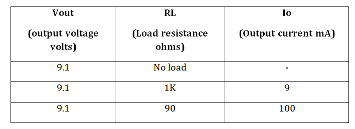
Fig. 7: Table listing the output voltage and current of the Adjustable Closed Loop Boost Converter for different loads with 60 percent duty cycle
Thus, it can be seen that a current of 100 mA can be consumed at the output with a tolerance limit of +/-0.5V.
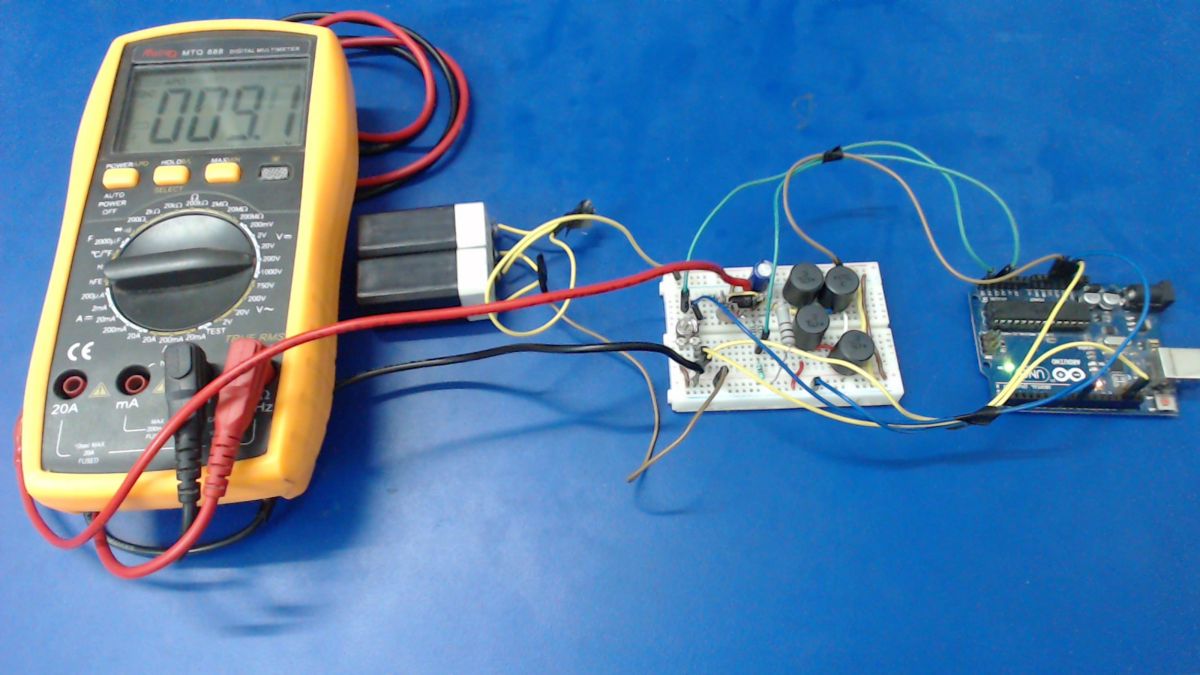
Fig. 8: Image showing the Closed Loop Boost converter under test
While measuring voltage and current values with different loads at the output when the duty cycle is set to 30 percent, the following observations were made –

Fig. 9: Table listing the output voltage and current of the Adjustable Closed Loop Boost Converter for different loads with 30 percent duty cycle
Thus, it can be seen that a current of 100 mA can be consumed at the output with a tolerance limit of +/-0.5V.
The power efficiency of the circuit can be calculated as follows –
For 60% duty cycle, the maximum output current is 100mA
Efficiency% = (Pout/Pin)*100(Power output) Pout = Vout*Iout
(Output voltage) Vout = 9.1 V
(Output current) Iout = 100 mA
Pout = 910 mW (approx.)
(Input power) Pin = Vin*Iin
(Input voltage) Vin = 3.7 V
(Input current) Iin = 270 mA (measure input current using ammeter)
Pin = 1000 mW (approx.)
Putting all the values,
Efficiency% = 90%
It can be seen that when using a feedback circuit, the efficiency of the boost converter increases from 89% (as calculated in the previous tutorial) to 90%.
This is a closed-loop boost converter with non-isolated output and operating in DCM mode. It can be used as a switching regulator for LED drivers and as a regulated DC power supply. It can be used to supply power to low-power portable electronic devices. In battery powered applications, when there is space constraint to stack number of batteries in series to achieve high voltage, this boost converter can be used with less number of batteries to supply DC power.
This boost converter is simple to design and uses inexpensive components. It can be easily assembled in a short time. The circuit has a variable output and can be powered by a 3.5V battery. However, the minimum battery voltage should not be less than 3.5 V, otherwise the microcontroller will not be powered.
Project source code
###
//Program to ////// Code for Closed Loop Boost converter with variable output voltage //////// ////// Output Voltage Adjustment from 5V to 9V //////// #define TOP 1599 // Fosc = Fclk/(N*(1+TOP)); Fclk = 16MHz, Fosc = 10kHz #define CMP_VALUE_HALF_DUTY 799 // 50% duty cycle #define FeedbackPin A4 // Input pin of potentiometer at A4 #define Inputpin A5 // feedback pin of potentiometer at A5 #define R1plusR2_resistor 6.0 // variable of R1+R2 value #define R1_resistor 1.0 // variable of R1 value #define PWM 9 // PWM(Pulse Width Modulation) wave at pin 9 //// function declaration float Map_feedback(float); //function to map feedback values float Mapping_output_voltage(float); //function to map potentiometer values void InitADC(void) ; // Function to start ADC conversion uint16_t ReadADC(uint8_t); // function to read Analog value ///// function definition //////// float Mapping_output_voltage(float Input_Read ){ float Compare_voltage = (((Input_Read*(1.0)/1024)*4)+5); // mapping the digital value into analog voltage from 5V to 9V return(Compare_voltage); // return the output calculated voltage } void InitADC(void){ ADMUX &= ~((1<Compare_voltage_input) //comparing actual output voltage with desired output voltage to find error in voltage { OCR1A --; // if error is positive the duty cycle is decreased } else if(actual_output_voltage < Compare_voltage_input) { OCR1A++; // if error is negative the duty cycle is increased } } ###
Circuit diagrams
| Circuit-Diagram-Adjustable-Closed-Loop-Boost-Converter |  |

