8.3) Voltage follower
The voltage follower is an op amp amplifier circuit with negative feedback. It acts as emitter follower configuration of transistor based amplifiers. They provide unity gain to the applied input signals. Unity gain means that the output voltage will be exactly equal in magnitude to the input voltage.
voltage follower
In the above figure, a non-inverting voltage follower is shown. The input voltage V1 is applied to the non-inverting pin of the operational amplifier. Here the feedback resistance Rf is zero, i.e. short circuit. The amplifier gain reduces from ideally infinite to unity.
If V1 is the input voltage at the inverting pin and V0 is the output voltage of the op amp, then V0 will be exactly equal to V1 in magnitude. Therefore, the gain is given by the following equation.
Gain=V0/V1= 1
Voltage follower is generally used to amplify the current of a signal while maintaining the same voltage in case of driving high output loads (low resistance circuits).
The things we discussed in this section can be summarized as follows;
Inverting amplifier and non-inverting amplifier are negative feedback operational amplifier circuits
Non-inverting amplifier, the input signal is applied to the non-inverting pin
Inverting amplifier, the input signal is applied to the inverting pin
Voltage follower is a negative feedback operational amplifier circuit with unity gain
(header = simple microphone amplifier)
8.4) Simple microphone amplifier
We have already discussed how negative feedback can be implemented for the purpose of designing practical amplifiers based on operational amplifiers. The concept of negative feedback, inverting and non-inverting configurations should be very clear before we proceed to this practical circuit.
The circuit is shown in Figure: 44 is a simple operational amplifier inverting amplifier. In this circuit, the feedback resistance Rf is represented by resistance R4 and R1 is introduced into the circuit by the impedance of capacitor C1.
The operational amplifier based microphone amplifier circuit is shown below.
Microphone amplifier
The microphone output will be in the range of a few millivolts. It must be amplified several times to make it useful for any practical use. In this circuit you can connect a microphone at one end and the amplified sound signals can be played by connecting a speaker at the other end.
The LM358 operational amplifier IC is also used in the above circuit. The microphone is pulled through a resistor. The sound signal is coupled to the microphone using a capacitor and applied to the inverting pin of the operational amplifier. A divider bias potential is given to the non-inverting pin. A feedback is also implemented using a resistor on the inverting pin. Hence, the circuit forms a negative feedback inverting amplifier. The amplified signal is coupled and sent to a speaker.
The output coupling capacitor is used to couple only the AC component, which is the actual signal. The output can be obtained directly from pin 1 also without coupling capacitor and can be used with other circuits. The output pin of the amplifier module is actually taken directly from the output of the LM358.
The picture of operational amplifier based microphone amplifier is shown below:
Microphone amplifier image
As you can see in the figure above, I made the circuit for a module, to which I can connect a microphone and a speaker. Additionally, the module has pins, so the entire module can be connected to a breadboard or other larger circuits. There are three pins, VCC, GND and OUTPUT. The OUTPUT pin is taken from pin 1 of the op amp without including the coupling capacitor. It can also be obtained through a resistor that can be connected and removed from the base of the IC whenever you want, as you can see in the image.
If you look at the image of the microphone amplifier, you can see a resistor at the base of the IC along with the LM358. Such an arrangement is made in such a way as to introduce any value of resistance whenever we need to connect the amplifier module to other circuits without output coupling capacitor
Component specifications:
R1=18KE, 1/4W resistor
R2=R3=1KE, 1/4W resistor
R4=560KE, 1/4W resistor
C1 = 0.1uf disk capacitor
C2=100uf, 16V electrolytic capacitor
SP1=8E, speaker
M1=microphone
Component Significance:
R1: The value of this resistor must not be too high, so that we can have sufficient voltage variations coupled to the amplifier, and not too low so that we can have enough current flowing into the amplifier.
R2 and R3: These resistors must have equal values so that we can fix the operating point in their center. This simply means that we can have a full amplified signal output for both positive and negative halves for a signal with equal positive and negative halves using this configuration.
R4: The value of R4 determines the gain of the circuit. When we increase the gain of R4 increases and when we decrease the gain of R4 decreases.
C1 and C2: C1 and C2 are coupling capacitors used to couple only the AC waveforms of the input microphone and output speaker respectively. Their values are calculated based on the frequency range of the input signals (in this case, human voice; ~3.5 KHz)
(header = op-amp based comparators)
9) Comparators based on operational amplifiers
In addition to amplification, operational amplifiers are widely used to compare two signals and produce a corresponding output. The working concept of the operational amplifier is similar to what we have already discussed in the section on level detectors in 7.2). The comparator is nothing more than a level detector, where we can predefine a reference voltage on one pin and the voltage to be compared on the other pin. The output produced depends on the pin to which you are applying the voltage to be compared.
The input voltage must be applied to the non-inverting pin for a comparator to produce high output whenever the input voltage is equal to or greater than the reference voltage, or to the inverting pin otherwise.

Operational Amplifier Comparator
The above circuit is an op-amp comparator in which the inverting pin is held at a reference voltage and the variable input signal is fed to the non-inverting input pin. Whenever the voltage at the non-inverting pin exceeds the voltage at the inverting pin, the output will be positive and negative.
Here +2V is supplied to the inverting input of the op amp, so as long as the Vin which is supplied to the non-inverting pin remains at lower voltage than +2V, the output will be negative (almost equal to -10V). Whenever Vin becomes equal to +2V, the output becomes positive (almost equal to +10V).
It should be kept in mind that even the minimum increment of Vin greater than Vref will trigger the output to positive and the minimum decrease of Vin less than Vref will trigger a negative output.
Suppose a sine wave is applied to Vin and has a DC content of exactly +2V, the input and output waveform of such a circuit condition is shown below.
Operational Amplifier Comparator Waveforms
Video
(heading = op-amp based comparators, continued)
There are commercial op amp ICs available which are specially made for comparison operations, in which even when equal input voltages can drive a positive output. There are ICs that have more than one comparator module in a single package. LM339 is an IC widely used in electronic devices.
LM339 is a 14-pin IC, which consists of four operational amplifiers within a single IC package. It can also work with single power supply like LM358. The pinouts of IC LM339 are shown in the following figure.
LM339 Pinouts
Those who would like to try the LM339 IC should note that the output of the LM339 is open drain, meaning the output pin comes from the collector of a transistor. The output transistor will only activate when it is connected to a VCC through your device.
Connecting LM339 to a device
In the figure above, the block mentioned as “DEVICE” can be anything like LED, motor or even a simple resistor.
That's all about the basics of comparators and comparator ICs, now let's try out some really interesting circuits in the following section that make use of the knowledge we've gained so far.
(header = voltage level indicator)
9.1) Voltage level indicator
A voltage level indicator is a very useful circuit to be used with various sensors with analog output. There are 8 raw LEDs that indicate 8 voltage levels in ascending order. The right end LED represents the minimum voltage and the left end LED represents the maximum voltage. As the voltage increases, the LEDs begin to glow from right to left.
I chose IC LM339 to design a voltage level indicator, the features of which we discussed in the previous section. It consists of four operational amplifier comparators. The IC has 14 pins, among which two of them are VCC and GND, and the rest of them are inverting and non-inverting pins and their respective output pins of the four operational amplifiers.
Two LM339 ICs are used in cascde and all non-inverting pins of both LM339 are shorted and connected to a common input point. A potential divider network of resistors is used to supply voltage to the inverting pins of the operational amplifiers in ascending order. Whenever the potential at the common input point increases more than the potential at the inverting pin of a particular op amp, its output increases and the LED connected to that output pin glows.
The voltage level indicator circuit diagram is shown in the following figure.
Voltage level indicator circuit
From the above circuit, resistors R9 to R16 along with variable resistor R17 form a potential divider network. The potential across the resistors can be adjusted by varying R17. If we assume that all nine resistors, including R17, have the same value, then the voltage across each resistor will be 5/9 volts. Therefore, the voltage at the inverting input of op amp U2_4 will be 5/9 V, op amp U2_3 will have 5/9 V + 5/9 V. i.e. (5/9) * 2, op amp U2_2 will have (5 / 9)*3 and so on. Finally, the op amp inverting pin U1_1 will have a potential (5/9)*8. Note that this condition is true only when the variable resistor is adjusted so that it has a resistance value equal to that of resistors R9 through R16. If we adjust the variable so that the resistance increases, the voltage across the individual resistors will decrease equally. If the variable resistor is adjusted so that its resistance decreases, the voltage across the individual resistors will increase equally.
The working of the circuit can be explained with the help of an example. Suppose all nine resistors, including R17, have the same value, then the voltage across each resistor will be 5/9 volts. Suppose an input voltage greater than (5/9)*3 is applied. As we mentioned before, this voltage is greater than the voltages on the inverting pin of U2_3, U2_2 and U2_1 and therefore produces high output and the corresponding three LEDs glow. Again, assume the input voltage is greater than (5/9)*8. Now all the non-inverting pins are at a higher potential than the inverting pins of both LM339s. Consequently, at this input voltage, all op amps produce high output and all LEDs glow.
Component specifications:
R1 to R16=1KE, 1/4W resistor
R17 = 100KE potentiometer
D1 to D8=LED 3mm
U1=U2=LM339
Component Significance:
R1 to R8: These resistors control the brightness of the LEDs. Resistors with a value above 220 ohms are safe for use with LEDs.
R9 to R16: These resistors adjust the voltage at the inverting pin of each comparator. All of these resistors must have equal values so that the output changes for an equal increase in input voltage each time.
R17: This variable resistor defines the sensitivity of the voltage level indicator circuit. When you increase the resistance, the voltage appearing at the inverting pins reduces equally, and as a result, changes in the output occur quickly and the input range that the circuit can detect decreases. If you decrease the resistance, the voltage appearing at the inverting pins increases equally, and as a result, changes in the output occur slowly and the input range that the circuit can detect increases.
The circuit in Figure: 57 is built in two separate modules and then joined together. It is always recommended for ease of assembly, debugging and hardware reuse. Hardware reuse means that we can use the same module, say display module, with some other larger circuit.
One of the modules has only LEDs and their current control resistors, and we can call this module a display module. I turned it into a module so it can be used with other larger circuits. The other module has the LM339 ICs and the resistor network.
The image of the two modules is shown in the following image.
Display module and comparator modules
You can see all eight LEDs, eight resistors, and nine pinouts on the display module. One of the pins is used for common positive supply and the rest of them can be connected to the output pins of op amps. This module can be plugged into a breadboard and then connected to the comparator module or directly to the comparator module, as the comparator module is built in such a way that it has connectors to house the display module.
Video
(header= Voltage level indicator Contd…)
In the comparator module there are two LM339 ICs, eight resistors, a variable resistor and a connector to house the display module. This module also has pinouts including VCC, GND, and INPUT so the entire module can be connected to a breadboard or other larger circuits.
The two modules can be connected together to form the voltage level indicator as shown in the following image.
Voltage Level Indicator
We can test the module by applying some external voltage from other devices if we have any, or simply apply a voltage using a variable resistor and observe the variations in the output in relation to the variations in the input voltage. Such an arrangement is shown in the following figure.
Voltage Level Detection Setting
The value of variable resistance R1 can be anything above 1K ohm. As we vary the resistance, we vary the voltage input to the voltage level indicator module. The module detects this voltage and the output LEDs glow accordingly.
The image of this voltage level indicator setting is shown in the following figure.
Voltage Level Detection Image
(header = volume indicator)
9.2) Volume indicator
The volume indicator found on large speaker amplifiers used to catch my attention. It's great to see the LEDs shining according to the volume of whoever is speaking through the microphone. Let's see how we can build our own simplest volume indicator.
The interesting thing is that the volume indicator can be realized by connecting the modules we have already made. This can be explained with the help of the following block diagram.
Volume indicator block diagram
As shown in the figure above, the sound amplifier module amplifies the sound signals from the microphone, feeding them to the comparator module, which then activates the LEDs according to the amplitude of the input signal. As the volume increases, the strength or amplitude of the signal input to the comparator module increases. Therefore, the louder the voice, the more LEDs shine on the display module.
Before we proceed with the connection, we need to make some adjustments to the microphone amplifier module. The speaker must be removed and the output must be taken directly from the output pin through a high value resistor. We have already made arrangements for the introduction of a resistor and the module's output pin taken directly from the LM358 output.
The modified circuit is shown in the following figure
Modified microphone amplifier circuit
The component specifications are the same as the previous circuit, except that there is an additional resistor R5 with a resistance value of 270K ohms.
The image of the actual connection made on the breadboard according to the block diagram in Figure: 53 is shown below.
Volume indicator image
Images of all the modules I built are shown in the following image. I recommend that the reader try the circuit first on the breadboard and, once it works, incorporate it into a module that we can connect to a breadboard later or into another larger circuit.
All modules
Video
(header= Operations on input voltages)
10) Operations at input voltages
Op-amp stands for Operational Amplifier, and received this name because it is capable of performing certain operations on the applied input voltages, in addition to just amplifying them. An operational amplifier is capable of adding and subtracting input voltages and amplifying the result. This type of operational amplifier circuit is often called a summing amplifier.
10.1) Summing amplifier
An operational amplifier can be configured in such a way that the sum of the voltages applied at the input can be obtained at the output with an amplification. Voltages applied to the non-inverting input pin are added and voltages applied to the non-inverting input pin are subtracted.
Operational amplifier based adder
The above circuit is an operational amplifier based voltage adder. Let's assume that the input resistance has the same values, that is, R1=R2=R3=R. Let the voltages applied to the inverting input pin be V1, V2 and V3. In this case, the output voltage can be calculated from the following equation.
Vout=-(Rf/R)(V1+V2+V3)
Now let's consider a voltage summing amplifier complete with voltage addition and subtraction capabilities. Input voltages are applied to inverting and non-inverting inputs.
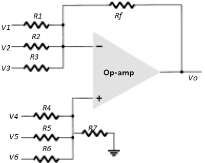
Operational amplifier based adder and subtractor
In the above circuit V1, V2 and V3 are the voltages applied to the inverting input and V4, V5 and V6 are the voltages applied to the non-inverting input. We assume that all resistors except Rf are equal. i.e. R1=R2=R3=R4=R5=R6=R7=R. In this circuit, the output voltage can be obtained by the following equation.
Vout=-(Rf/R)(V1+V2+V3-V4-V5-V6)
The summing amplifier has many practical applications. This application involves mixing signals in amplifiers. They are also used in analog signal processing and were widely used in early analog computers.
What I have been trying to convey through this article is presented below;
Op-amp is an electronic circuit, made of basic electronic components. This circuit is capable of performing certain operations on the input signals, in addition to amplifying them.
So far we have seen some basic circuits using operational amplifiers and I suggest the reader to analyze the topics in detail. Practice as many circuits as possible. With each circuit you learn something new about the operational amplifier and your knowledge becomes more solid. The operational amplifier is an interesting electronic device and believe me, you will enjoy making circuits with it!