In the previous tutorial, it was discussed how arithmetic operations on binary numbers can be implemented through Boolean logical operations. In a digital circuit, logical operations are performed by logic gates. A logic gate is an electronic circuit that makes logical decisions. AND, OR and NOT are the basic logic gates.
NAND and NOR gates are derived from them. Any computing problem in digital circuits can be expressed by a Boolean equation or Boolean expression. A Boolean expression can be minimized to Minterms or Maxterms, reducing the expression to a two-level implementation that can be designed with NAND or NOR gates. This is why NAND and NOR gates are called universal gates. Exclusive OR gates are another logic gate that can be constructed using basic gates such as OR and NOT gates.
Logic gates can have two or more inputs and only one expected output for the NOT gate, which has only one input. The output signal of a logic gate appears only for certain combinations of the input signals, as the number of combinations is always limited by the number of Boolean variables (where each Boolean variable represents an input channel).
So basically, logic gates are the building blocks of a digital circuit that can perform basic manipulation of binary information. Any digital IC contains nothing more than an interconnected network of logic gates. Each gate is represented by a distinct logical symbol and its operation can be described using an algebraic function. The relationship between the input and output variables of each gate can be represented using a truth table and the signal response of any logic gate can be represented by the timing diagram. So let's learn about various logic gates.
OR Gate –
The OR gate performs logical addition, commonly known as the OR function. The OR gate has two or more inputs and only one output. The operation of the OR gate is such that HIGH(1) at the output is produced when any of the inputs is HIGH(1). The output is LOW (0) only when all inputs are LOW (0). Suppose, if A and B are the input variables of an OR gate and Y is its output, then
S = A + B
Similarly, for more than two input variables, the output of the OR gate can be expressed as follows –
Y = A + B + C + D +……
An OR gate constructed with diodes is shown below, in which A and B represent the inputs and Y the output. Resistance RL is the load resistance. The logic symbol of OR gate is also shown below –

Fig. 1: Image showing the OR gate symbol and circuit
If A = 0 and B = 0, both diodes will not conduct, therefore the output Y = 0. If A = 1 and B = 0, diode D1 conducts, therefore the output Y = 1. If A = 0 and B = 1, diode D2 conducts, therefore the output Y = 1. If A = 1 and B = 1, both diodes conduct and therefore Y = 1. The output of an OR gate for two Boolean variables can be represented by the following truth table –
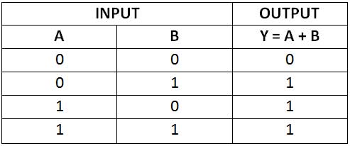
Figure 2: OR gate truth table
The truth table for the OR gate can be represented graphically by the following timing diagram –

Fig. 3: OR gate timing diagram
And Gate –
The AND gate performs logical multiplication, commonly known as the AND function. The AND gate has two or more inputs and a single output. The operation of the AND gate is such that HIGH (1) occurs only when all inputs are HIGH (1). Even when one of the inputs is 0, the output will be zero. Suppose, if A and B are the input variables of the AND gate and Y is its output, then
S = A · B
The dot (·) denotes the AND operation, but can usually also be written as Y = AB. The two input AND gates constructed using the diodes are shown below, in which A and B represent the inputs and Y the output. The logical symbol of AND gate is also shown below –
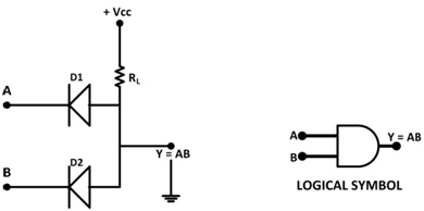
Fig. 4: Image showing the AND gate symbol and circuit
If A = 0 and B = 0, both diodes conduct because they are forward biased, therefore the output Y = 0. If A = 0 and B = 1, diode D1 conducts because they are forward biased and therefore the output Y = 0. If A = 1 and B = 0, diode D2 conducts because it is forward biased, and therefore output Y = 0. If A = 1 and B = 1, both diodes do not conduct because they are reverse biased, and, therefore, the output Y = 1. The output of an AND gate for two Boolean variables can be represented by the following truth table –

Fig. 5: AND Gate Truth Table
The truth table for the AND gate can be represented graphically by the following timing diagram –

Fig. 6: AND gate timing diagram
NO Gate –
The NOT gate performs the basic logical function called Inversion or complementation. The purpose of this gate is to convert one logic level to the opposite logic level. It has an entrance and an exit. When the High level is applied at the input, the low level appears at the output and vice versa. A NOT gate constructed using a transistor is shown below, where A represents the input and Y represents the output. The logic symbol of the NOT gate is also shown below –
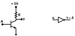
Fig. 7: Image showing the NOT gate symbol and circuit
When the input is HIGH, the transistor is in the ON state and the output is LOW. When the input is LOW, the transistor is in the OFF state and the output is HIGH. The output of a NOT gate can be represented by the following truth table –
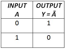
Fig. 8: NOT Gate Truth Table
The truth table for the NOT gate can be represented graphically by the following timing diagram –
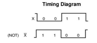
Fig. 9: NOT gate timing diagram
NAND gate –
NAND gate performs the logic function which is the serial combination of NOT and AND gates. It has two or more inputs and only one output. The logic symbol for NAND gate is shown below –

Fig. 10: Image showing the NAND gate symbol and circuit
In a NAND gate, when all inputs are HIGH, the output is LOW. When either input is LOW, the output is HIGH. The output of a NAND gate for two Boolean variables can be represented by the following truth table –
Fig. 11: NAND Gate Truth Table
The truth table for the NAND gate can be represented graphically by the following timing diagram –
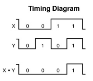
Fig. 12: NAND gate timing diagram
NOR Gate –
NOR gate performs the logical function which is the serial combination of NOT and OR gates. It has two or more inputs and only one output. The logic symbol for the NOR gate is shown below –

Fig. 13: Image showing the NOR gate symbol and circuit
In a NOR gate, when all inputs are LOW, the output is HIGH. When either or both inputs are HIGH, the output is LOW. The output of a NOR gate for two Boolean variables can be represented by the following truth table –

Fig. 14: NOR Gate Truth Table
The truth table for the NOR gate can be represented graphically by the following timing diagram –

Fig. 15: NOR gate timing diagram
EXCLUSIVE OR ( Ex – OR ) Gate –
An exclusive OR gate is a gate with two or more inputs and outputs. The output of a two-input are HIGH or LOW. The logical symbol of XOR is shown below –

Fig. 16: Image showing the XOR gate symbol and circuit
The output of an XOR gate for two Boolean variables can be represented by the following truth table –

Fig. 17: XOR Gate Truth Table
The truth table of the XOR gate shows that the output is HIGH when any but not all of the inputs are 1 and when both inputs are equal, i.e. 0 or 1, the output is LOW. This unique feature eliminates the similarity with the OR gate. The truth table for the XOR gate can be represented graphically by the following timing diagram –
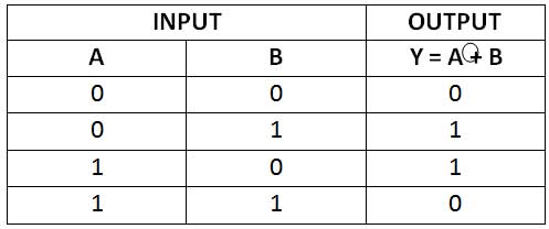
Fig. 18: XOR gate timing diagram
Exclusive – NOR Gate (XNOR) –
The XNOR gate performs the logic function which is the serial combination of NOT and XOR gates. The output of an XNOR gate assumes a HIGH state if all inputs assume the HIGH state or the LOW state. If any of the inputs have a different logic state, the XNOR gate output will be LOW. The logical symbol of XNOR is shown below –

Fig. 19: Image showing the XNOR gate symbol and circuit
The output of an XNOR gate for two Boolean variables can be represented by the following truth table –

Fig. 20: XNOR Gate Truth Table
The truth table for the XNOR gate can be represented graphically by the following timing diagram –
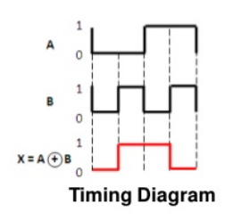
Fig. 21: XNOR gate timing diagram
These logic gates are the building blocks of any digital circuit. In the next tutorial, learn about Boolean algebra theorems and how a Boolean expression can be minimized to Minterms and Maxterms, hence it can be implemented by interconnecting two levels of universal logic gates (NAND and NOR).

