October 6, 2009, Stockholm, It was a historic moment for digital cameras when their shutters opened for a split second to capture the committee, awarding the coveted Nobel Prize to those who invented electronic eyes. If it weren't for the duo of Willard Boyle and George Smith, these cameras might still be illuminating photosensitive film and then drying it on rails in the darkroom. By inventing the Charge Coupled Device and envisioning its applications in 1969, Boyle and Smith opened the realm of solid-state devices for imaging and memory applications.

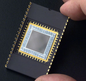
Figure 1: An image of the charge-coupled device
Although Boyle and Smith invented the method for converting light into an electrical signal, all of the research would not have been possible if not for Albert Einstein's groundbreaking explanation of the photoelectric effect. Einstein explained how materials could absorb incoming radiation and the eventual elimination of electrons from the surface. Boyle and Smith studied how this incidence of light caused disturbances in electrons and how it could be used. They managed to do this by grouping several capacitors together in an array, something that makes up the pixels of a digital image.
Initially named as Load Bubble Devices , the device's operation as a shift register and linear imaging device was recorded. It was based on a similar principle to Bucket-Brigade devices, where charge is transferred from one capacitor to another along the semiconductor surface. Bell Labs managed to build the first solid-state video camera in 1970. In 1971, Michael F. Tompsett and other researchers at Bell Labs were able to capture images with linear imaging. CCD matrices . After that, many semiconductor companies like Texas Instruments, Fairchild Semiconductors, Sony etc. CCD Technologies . One of the first commercial CCD devices was built by Fairchild in 1974, which was a 100x 100 pixel device with about 500 CCDs. The first CCD-based reconnaissance satellite KH-11 KENNAN was launched in 1976. In 1983, CCDs began to replace photographic plates in astronomical telescopes as well. Companies like Kodak had been manufacturing professional CCD-based cameras since 1985, but in 1995, high-resolution, cost-effective CCD cameras began flooding the markets.
A CCD can be thought of as a subset of charge transfer devices. They are based on Metal Oxide Semiconductor (MOS) capacitors. Two types, surface channel and buried channel MOS capacitors, have been used in CCD, but mostly buried channel capacitors have been used for manufacturing since they have no problems caused by irregularities surface at the oxide-semiconductor interface. A thin buried n-type channel is formed on a p-type substrate through ion implantation. The insulating silicon dioxide layer is grown on top of the ne region, to complete the capacitor, metal gates or heavily doped polycrystalline silicon are placed on top of the insulating SiO. 2 using CVD process. To isolate the charge packets of one column from the other, thermally grown oxide 'channel stops' are placed parallel to the channels.

Figure 2: Graphical image of the buried channel MOS capacitor
But if a CCD cell transmitted charges, it would be just any other MOS capacitor. The additional property of being sensitive to light makes the CCD unique. The response to photons occurs through the epitaxial layers of doped silicon that grow on the substrate. When photons strike the surface of the semiconductor, they dislodge electrons which create a charge that is proportional to the light falling on the surface. A single CCD cell performs four functions:
1. Receive charge from the cell above it in the array.
2. Keep this charge for some time without much loss.
3. Pass this charge to the cell below it in the matrix.
4. Respond to external stimuli such as light and generate your own charge.
Elements and Cont. of Work.
Therein lies the main challenge: reading these accusations. Many schemes called binning, two-phase, three-phase, four-phase, etc., corresponding to the type of clock used, were used to transfer the payload packets from cell to cell in a bucket brigade style, protecting the integrity of each packet. Considering a three-phase scheme, there would be 3 control wires passing through each cell, with each wire connected to a phase of the clock. These wires control the height of the potential wells that push and pull the load packets along the line. For a three-phase scheme, each pixel contains one storage and two barrier ports. Each storage port is connected to the same phase and sequentially, each barrier port is connected to their respective phase clocks. A charge packet moves from one region to the next region when the second port goes to a higher potential and the first port goes low. This sequential movement of loads can be demonstrated as in the figure below.

Figure 3: Graphic Figure of the Sequential Movement of Charges in the CCD
Attempts have been made to use CCD devices as memory devices. But soon after, other techniques took over and after that CCD devices were mainly used in scanning, microscopy and photography. The one-dimensional array has been used in flatbed scanners where one line is scanned at a time and charges are read after that. The matrix is mechanically moved across the page to create two-dimensional scanned images. Two-dimensional arrays were used to capture the entire scene at once and then transfer the charges to the output.

Fig. 4: A one-dimensional array image
Architecture
To read the CCD set, three architectures were used:

Figure 5: Diagram showing the Full Frame CCD architecture
1. Full Frame Reading: The entire CCD array acts as an active area. This type of device uses a mechanical shutter mechanism to block light from reaching the element, preventing smearing when charges are passed through the vertical CCDs in parallel and subsequently moved in series using the horizontal CCDs. This process is quite time-consuming.

Figure 6: Graphic image representing/diagram showing frame transfer CCD architecture
Architecture Cont.
2. Frame transfer: Half of the contiguous area of the matrix is used for exposure and the remaining half is opaque. Charges are transferred from the active area to the opaque area in much less time and are then read from there. This process is faster than reading the full frame because during the time charges are being read in the opaque area, the active area can be used to capture a new image. It also has the advantage of reducing stains and light contamination during cargo transfer. However, this has the disadvantage of using twice the silicon area.

Figure 7: Graphical image representing/diagram showing inter-line transfer CCD architecture
3. Interline Transfer: In this type of architecture, each pixel has an active area and an opaque area adjacent to it. Charge is rapidly transferred from the light-sensitive photodiode to the adjacent vertical CCD unit. This uses just one transfer cycle to hide the entire image, thus allowing for very high shutter speeds and minimal blur. This also has the disadvantage of increasing the state of the silicon, but modern advances have attempted to increase the quantum efficiency of the array using microlenses that redirect light away from opaque regions. The use of microlenses increased the fill factor to around 90% of other architectures without compromising speed.
Working
The main performance parameters of a CCD device are speed, sensitivity, resolution and cost. However, the choice of architecture depends on the application of the devices. Although astronomy requires maximum light to be captured, price is rarely a constraint, full frame readout architecture CCD devices are used. But in the case of point-and-shoot cameras, where shutter speed and cost are more important, the interline architecture is the most popular.
CCD matrices are only sensitive to intensity and not color. So, to obtain a colorful image, filters are used. Color images can be obtained using the Bayer Pattern or 3CCD and a dichroic beam splitter prism.

Figure 8: Representative image of the Bayer pattern
Bayer Pattern is a special color grid that is placed over the image matrix. Since human eyes are more sensitive to the color green, two out of every four grids have a green filter. The others have blue and red, making up the RGB color pattern. A digital signal processor interpolates the two missing colors from neighboring pixel values. The Bayer pattern, although simple and cheap, throws away information compromising the image resolution. Additionally, when used in locations with abrupt changes in light intensity, the Bayer pattern creates artifacts. Some cameras may also use different color patterns for color generation. Resolution can be improved in specific applications by Microscanning technology.
A dichroic beam splitter prism divides the image into red, green and blue components which can then be incident separately on three CCD devices. This offers greater quantum efficiency compared to the Bayer mask, as most of the light is captured by the sensors and not absorbed by the mask's intermediate layers. These devices have been used in professional video camcorders.
A CCD device, despite all the good features it has to offer, also has some disadvantages. Coupling charges along a row of many pixels results in the loss of a considerable amount of charge, resulting in fading. Improper shutter control or excessive bright conditions that lead to too many photons hitting the CCD element result in charge leakage to the neighboring pixel, which causes blooming.
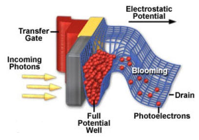
Figure 9: Graphic image representing the operation/diagram showing the operation of the dichroic beam splitter prism
Furthermore, if photons hit the sensors while charge is being transferred due to improper clocking, data loss in the form of smears may occur. The sensitivity of a CCD device is often a function of the operating temperature. As the temperature increases, the dark leakage current also increases, thus reducing sensitivity. Noise is inherent in all electronic equipment and in the case of CCD-based devices, SNR degradation can occur due to photon noise, dark noise or readout noise or a combination of these. However, intensive research work in this field has produced positive results and the development of many improved variants. Devices such as electron multiplication CCDs (EMCCDs), which incorporate on-chip multiplication gain, have helped achieve single-photon detection sensitivities without compromising the resolution or efficiency of the CCD structure, while also reducing costs. These characteristics are typical of expensive electron-bombarded CCDs, which use an image intensifier with a CCD device.
CCD x CMOS
There has been direct competition between CCD and CMOS imaging technologies. CCD and CMOS imaging were invented around the same time within a few years. However, CCDs became dominant due to the superior results of the manufacturing technology then available. CMOS technologies focused on uniformity and smaller feature sizes, which did not happen until the 1990s when lithography advanced enough to support small feature sizes. It was after this that CMOS imagers made a comeback, and since then both technologies have fought for market dominance. While CCD sensors are known to offer the best image qualities, CMOS imagers offer more on-chip functions and attractive features such as lower power consumption, making them more popular in mobile phone cameras, etc. Decision will be made depending on application requirements.
|
Factor
|
CCD
|
CMOS
|
|
Responsiveness
|
Moderate
|
Higher
|
|
Dynamic Range
|
High
|
Moderate
|
|
Uniformity
|
High
|
Low
|
|
Speed
|
Moderate
|
Higher
|
|
Anti-bloom
|
High
|
High
|
|
Signal outside the pixel/chip
|
Electron Packet/Voltage
|
Voltage/Bits
|
|
System/sensor complexity
|
Tall short
|
Low High
|
|
Noise
|
Low
|
High
|
Markets have seen a rapid decline in the share of CCDs due to the growing popularity of CMOS sensors in cell phones and point-and-shoot cameras, and even industry stalwarts like Canon and Sony, which primarily used CCD products, are now moving to CMOS imagers. . It is expected that more than 95% of the camera market will switch to CMOS sensors by 2014. But it still remains and will continue to be a predominant segment that will continue to rely on CCD sensors, scientific research and the astronomer community, the biggest example being the Hubble Space Telescope. So even though light from CCDs may be disappearing from Earth, we would still need a CCD to see what's out there.