A tunnel diode – also called an Esaki diode because Leo Esaki invented it in 1957 – is a heavily doped PN junction diode that exhibits negative resistance and high conductivity due to the tunneling effect. In signal diodes (small signal diodes and rectifier diodes), the charge carriers gradually overcome the depletion region. In a tunnel diode, the charge carriers spontaneously overcome the barrier.
Another distinct feature of tunnel diodes is their negative resistance. A tunnel diode conducts in both directions, and the current through the diode decreases with increasing voltage.
The concentration of impurity atoms in a typical signal diode is one part in 10 8 . While in a tunnel diode, the concentration of impurity atoms is one part in 10 3 . Due to the strong doping of the depletion region, a tunnel diode is highly conductive in the forward and reverse bias regions. Its conductivity changes spontaneously, making it suitable for high-frequency switching. This is why tunnel diodes are used as high-speed switches as well as high-frequency amplifiers and microwave oscillator circuits.
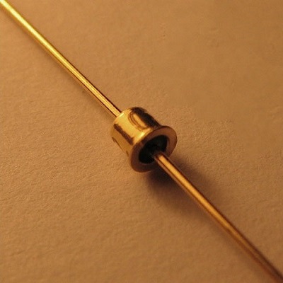
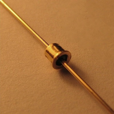
Tunnel diode example
Tunnel diode symbol
The tunnel diode is shown below in a circuit using one of two electrical symbols.
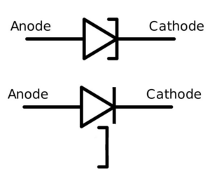
Tunnel diode electrical symbols
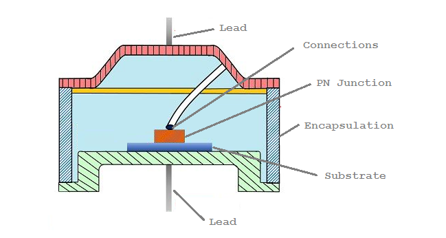
Tunnel diode construction
Unlike typical signal diodes, tunnel diodes are not constructed of silicon. The materials used in the construction of a tunnel diode are gallium antimonide, gallium arsenide, and germanium. In a tunnel diode, as forward voltage is applied, the current spontaneously increases to a peak value and, as the voltage increases, it reduces to a minimum level called the valley point. The ratio of peak current to valley current is very small in the silicon substrate, so it is not appropriate to build a tunnel diode; however, the ratio of peak current to valley current is maximum in case of germanium.
In addition to material selection, the second important factor in constructing a tunnel diode is the doping level. The heavily doped PN junction is almost 1000 times larger than that of a normal diode. The depletion region in a tunnel diode becomes extremely narrow due to this strong doping.
Tunnel diode electrical symbols
Tunnel diode VI characteristics
Just like a semiconductor diode, a tunnel diode is also a two-terminal device. Voltage can be applied to a tunnel diode in forward or reverse bias. When a forward voltage is applied to a tunnel diode, the current through the diode begins to increase spontaneously due to the tunneling effect. This is called tunneling current. It instantly reaches a maximum value called the peak point. The voltage at the peak point is called peak voltage and the current is called peak current. This is the maximum current that the tunnel diode can conduct.
As the voltage increases, the current through the tunnel diode begins to drop. It slowly reduces to a minimum value called valley current. This is called the reverse resistance region of the tunnel diode. The relationship between peak current and valley current is most significant in the switching operation of a tunnel diode. The peak current and valley current of some common tunnel diodes are listed in the table below.

After reaching the valley point, the current increases as the voltage increases, similar to a large signal diode. The voltage at the point where the current recovers to one-quarter of the peak point current is called the forward saturation voltage ( VFS ). The current increases until a maximum forward voltage is reached.
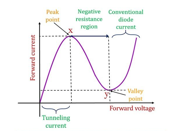
Tunnel diode VI characteristics
When a reverse bias is applied, the tunnel diode conducts a high value of reverse saturation current due to strong doping – it breaks down like a normal diode on a reverse voltage spike. The peak inverse voltage of all tunnel diode models listed above is 40V.
Tunnel Diode Equivalent Circuit
Tunnel diodes are used as high-speed switches. The most significant characteristic of a tunnel diode is its negative resistance region. The conductivity drop in the negative resistance region of a tunnel diode determines its switching operation. This is why, for circuit analysis of a tunnel diode, you use a small-signal diode model with negative resistance. The following is an equivalent circuit of a tunnel diode.
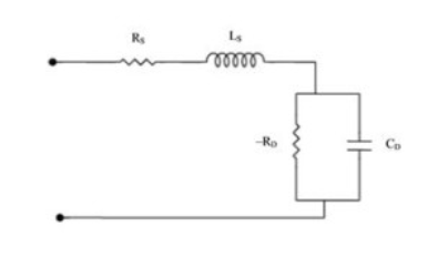
Equivalent circuit of a tunnel diode
In the equivalent circuit above, -Ro is the diode resistance in the negative resistance region, Ls is the series inductance due to the terminals, and C is the junction capacitance.
How a tunnel diode works
In a typical signal diode, the depletion region is wide enough to prevent free charge carriers from passing through it. Under unbiased conditions, the electrons passing from the n-type region to the p-type region and the holes passing from the p-type region to the n-type region are minority charge carriers present in the depletion region. In a tunnel diode, the depletion region is very narrow, so that even most charge carriers can pass through the depletion region to the other sides. There is practically no depletion region between the p-type and n-type regions. In other words, we can say that the conduction band and valence band overlap in a tunnel diode.
Under impartial conditions, electrons and holes gain kinetic energy due to temperature and move freely across the junction. However, the electron and hole current are equal and cancel each other out. No net current flows through the diode in an unbiased condition. When a small forward voltage is applied to the tunnel diode, it is not able to overcome the potential barrier of the narrow depletion region. Still, some majority charge carriers can cross the depletion region due to the tunneling effect. This causes a small amount of direct current to pass through the diode.
As the voltage increases, the tunnel current begins to increase rapidly due to the free movement of charge carriers. The valence band of the n-type region overlaps with the conduction band of the p-type region, leading to an increase in current. As the voltage increases, more electrons and holes are generated, causing a high current to flow through the diode. Current flow also changes the valence band and conduction band energy levels of both regions. The current reaches a peak point when the valence band of the n-type region is equal to the conduction band of the p-type region.
Any further increase in voltage creates a strong electrostatic field due to the ions present in the depletion region. This causes misalignment of the valence and conduction bands, resulting in a drop in current through the diode. The current drops to a valley point where it is minimal. When the forward voltage further increases, the overlap of the valence and conduction bands completely decreases and the tunnel diode starts to behave like a normal diode.
A significant amount of reverse saturation current flows through the diode due to the tunneling effect under reverse bias conditions. The tunnel diode remains in reverse biased conduction state due to the large reverse current and due to strong doping, the peak reverse voltage is small compared to the maximum forward voltage. For example, the tunnel diodes listed in the table above have a maximum forward voltage of up to 500 V; the PIV rating for all of them is just 40V.
Advantages of tunnel diode
They are durable, low-cost devices suitable for high-frequency and high-speed applications. They are easy to manufacture and offer high-speed switching operation with low signal noise.
Disadvantages of the tunnel diode
Tunnel diodes are low power devices and exhibit fluctuation in the output voltage. Like any diode, the output and input circuit of a tunnel diode cannot be isolated as a two-terminal device. It is also not possible to manufacture tunnel diodes on a large scale.
Tunnel diode applications
A tunnel diode is a low-power device that is not often used in electronic circuits. Due to high speed switching operation, they are used in small current high frequency applications. The negative resistance region of the tunnel diode is used to design oscillator and reflection amplifier circuits. Since the tunnel diode remains in the conducting state in both forward and reverse bias, it is also used as a frequency converter. In digital circuits, these diodes are used as logical memory storage.