What is a diode?
A Diode is the simplest two-terminal single-sided semiconductor device. It allows current to flow in one direction only and blocks current flowing in the opposite direction. The two terminals of the diode are called the anode and cathode. The diode symbol is as shown in the figure below.
Figure 1: Symbol of a Diode
The characteristics of a diode closely correspond to those of a switch. An ideal switch when open does not conduct current in either direction and when closed it conducts in both directions. The characteristic of a diode is as shown in the figure below.

Figure 2: Graph showing the electrical characteristics of an ideal diode
Ideally, in one direction indicated by the arrowhead the diode should behave as short-circuited and in the other direction opposite to the direction of the arrowhead it should be open-circuited. By ideal characteristics, the diodes are designed to meet these features theoretically, but it is not achieved in practice. So the practical characteristics of the diode are just close to the desired one.
Figure 3: Chart display comparison of electrical characteristics of Ideal and Practical Diodes
How do diodes work?
The diode operates when a voltage signal is applied to its terminals. Applying a DC voltage to make the diode operate in a circuit is called 'biasing'. As already mentioned above, the diode resembles a one-way switch, therefore it can be in a conducting state or in a non-conducting state. The 'ON' state of a diode is achieved by 'forward bias', which means that a positive or higher potential is applied to the anode and a negative or lower potential is applied to the cathode of the diode. In other words, the 'ON' state of the diode has the current applied in the same direction as the arrowhead. The 'OFF' state of a diode is achieved by 'Reverse Bias', which means that a positive or higher potential is applied to the cathode and a negative or lower potential is applied to the anode of the diode. In other words, the 'OFF' state of the diode has the current applied in the opposite direction of the arrow tip.
During the 'ON' state, the handy diode offers a resistance called 'forward resistance'. The diode requires a forward bias voltage to switch to the 'ON' condition, which is called cut-off voltage. The diode starts conducting in reverse bias mode when the reverse bias voltage exceeds its limit, which is called breakdown voltage. The diode remains in the 'OFF' state when no voltage is applied to it.
A simple p-n junction diode is manufactured by doping pen-type layers onto a silicon or germanium wafer. Germanium and silicon materials are preferred for manufacturing diodes because:
· They are available in high purity.
· A slight doping, such as one atom per ten million atoms of a desired impurity, can change the conductivity to a considerable level.
· The properties of these materials change with the application of heat and light and are therefore important in the development of heat and light sensing devices.
Types of diodes
Types of diodes:
The other variant of diodes has different construction, characteristics and applications. The different types of diodes are:
· Small signal or small current diode – These diodes assume that the operating point is not affected because the signal is small.
· Large signal diodes – The operating point on these diodes is affected because the signal is large.
· Zener Diodes – This diode works in reverse bias condition when the voltage reaches the breakdown point. A stable voltage can be achieved by placing a resistor on it to limit the current. This diode is used to provide reference voltage in power supply circuits.
· Light Emitting Diodes (LED) – This is the most popular type of diode. When it works in forward bias condition, the current flows through the junction to produce the light.
· Photodiodes – Electrons and holes are generated when light hits the p-n junction, causing current to flow. These diodes can function as photodetectors and are used to generate electricity.
· Constant Current Diodes – This diode maintains constant current even when the applied voltage keeps changing. It consists of JFET (junction – field effect transistor) with the source shorted to the gate to function as a two-terminal current limiter or current source.
· Schottky Diode – These diodes are used in RF applications and fixture circuits. This diode has lower forward voltage drop compared to silicon PN junction diodes.
· Shockley Diode – This is a four-layer diode, also known as a PNPN diode. This didoe is similar to thyristor where the gate is disconnected.
· Pitch Recovery Diodes – This semiconductor diode has the ability to generate short pulses and is therefore used in microwave applications as a pulse generator.
· Tunnel Diodes – This diode is heavily doped in forward bias condition which has a negative resistance at extremely low voltage and a short circuit in the negative bias direction. This diode is useful as a microwave amplifier and in oscillators.
· Varator Diodes – This diode works in reverse bias condition and restricts the flow of current through the junction. Depending on the amount of polarization, the width of the depletion region continues to vary. This diode is composed of two plates of a capacitor with the depletion region between them. The variation in capacitance depends on the depletion region and this can be varied by changing the reverse bias in the diode.
· PIN diodes – This diode has an intrinsic semiconductor sandwiched between the P-type and N-type region. Doping does not occur in this type of diode and, therefore, the intrinsic semiconductor increases the width of the depletion region. They are used as ohtodiodes and radio frequency switches.
· LASER Diode – This diode produces laser-like light and is expensive compared to LED. They are widely used in CD and DVD drives.
· Transient Voltage Suppression Diodes – This diode is used to protect sensitive electronic components from voltage spikes.
· Gold-doped diodes – These diodes use gold as a dopant and can operate at signal frequencies even if the forward voltage drop increases.
· Super barrier diodes – They are also called rectifier diodes. These diodes have the property of low reverse leakage current like that of normal p-n junction diode and low forward voltage drop like that of Schottky diode with ability to handle surges.
· Point contact diodes – The construction of this diode is simpler and is used in analog applications and as a detector in radio receivers. This diode is constructed of n-type semiconductor and few conductive metals placed to come in contact with the semiconductor. Some metals move toward the semiconductor to form a small region of p-tpye semiconductor near the contact.
· Peltier diodes – This diode is used as a heat engine and sensor for thermoelectric cooling.
· Gunn Diode – This diode is made of materials such as GaAs or InP that have a region of negative differential resistance.
· Crystal diode – These are a type of point contact diode, also called a Cat whisker diode. This diode is made up of a thin, sharp metal wire that is pressed against the semiconductor crystal. The metallic wire is the anode and the semiconductor crystal is the cathode. These diodes are obsolete.
· Avalanche Diode – This diode conducts in reverse bias condition where the reverse bias voltage applied across the p-n junction creates an ionization wave which leads to the flow of large current. These didoes are designed to break at specific reverse voltage to avoid any damage.
· Silicon Controlled Rectifier – As the name suggests this diode can be controlled or driven to ON condition due to the application of small voltage. They belong to the thyristor family and are used in various areas of DC motor control, generator field regulation, lighting system control and frequency inverters. This is a three-terminal device with anode, cathode and third conductor or controlled gate.
· Vacuum Diodes – This diode is a two-electrode vacuum tube that can tolerate high reverse voltages.
Figure 4: Image showing symbols of various types of diodes
Figure 5: Image showing various types of diodes
Generic diodes (small signal and large signal):
A p-n junction diode is the simplest semiconductor device. It is a unilateral, bipolar, two-terminal rectifier device that conducts in one direction only. Generic diodes are used in the following fields:
· Rectification in power supply circuits
· Extraction of modulation from radio signals in a radio receiver and in protection circuits where large transient currents may appear in low-current transistors or ICs interfacing with relays or other high-power devices.
· Used in series with power inputs for electronic circuits where only a negative or positive polarity voltage is desired.
Figure 6: Image showing the construction of a generic diode
Construction
Construction:
A simple p-n diode is a junction where p-type and n-type layers are doped onto a silicon or germanium wafer. A p-type semiconductor is formed by doping trivalent impurity atoms or acceptors into pure silicon or germanium, thus having an excessive concentration of holes. An n-type semiconductor is formed by doping pentavalent atoms or donor impurities into pure silicon or germanium, thus having an excessive concentration of electrons. Therefore, holes are the majority charge carriers in a p-type region, while electrons are in the n-type region. Electron-hole pairs are thermally generated in both types, which constitute the minority charge carriers. It is notable that a p-type material has no positive charge despite having excessive holes, while an n-type material has no negative charge despite having excess electrons. This is because in a p-type material along with holes, anions are generated and the total number of protons and electrons still remains the same. This is similarly observed for n-type material.
The addition of an n-type pe doping onto a silicon or germanium wafer produces a small region on the order of micrometers that is depleted of free charge carriers. This region is formed due to the diffusion of holes from a p-type material and electrons from an n-type material, called the depletion region or space charge region or transition region. The p-type region to the left of the depletion region has a layer of acceptor negative ions and to the right is a layer of donor positive ions that induces an electrical flow or potential difference across the junction. The charge concentration is positive to the left of the junction and negative to the right of the junction. This potential barrier prevents holes from migrating to the n-type region and electrons from migrating to the p-type region as the potential increases for the holes and electrons will allow migration to the p-type and n-type regions. The charge-bearing regions surrounding the depletion regions are also called uncovered regions. This is shown in the graph below.

Figure 7: Linear Dioe Rating Chart and Step Graded Diode
It is also important that the minority load currents, that is, the electron current in the p-type region and the hole current in the n-type region, decrease exponentially along the length of the diode. The minority current is due to thermally generated and temperature-dependent electron-hole pairs. These currents are very small in magnitude, on the order of microamperes. However, in the conducting state, the current through the diode crystal remains stable. The total current is a sum of the minority and majority load currents due to the bipolar nature of the diode. Most charge currents are hole current in p-type and electron current in n-type are reduced as they migrate near the junction due to recombination. The minority currents are the electron current in the p-type and the hole current in the n-type are maximal near the junction and reduce as they migrate away from the junction as an exponential function. Most of the charge currents in their regions after crossing the junction are diffusion currents, while before the junction they are drift currents.
Ohmic contacts concept – In addition to the PN junction diode, there are two metallic semiconductor junctions originating from the conductors to connect the device. It is assumed that the resistance of these metal semiconductor contacts remains constant despite the magnitude and direction of the current. During diode operation, the applied voltage is only effective to increase or decrease the height of the PN junction potential barrier.
Note: Using a stepped diode may improve diode performance.
Principle and Operation
Principle and Operation:
Possible configurations for a diode are:
1. Open circuit
2. Short circuit
3. Direct trend
4. Reverse bias
1. Open circuit: In open circuit condition, the current flowing through the diode is zero (I = 0). The potential barrier at the PN junction remains the same as that created when manufacturing the diode.
Figure 8: Image showing diode operation in open circuit configuration
2. Short circuit: In the short circuit condition, the sum of voltages in the circuit must be zero. Therefore, it is assumed that the potential barrier at the PN junction is compensated by the potential drops at the metal semiconductor junctions. The holes provided by region n must be directed to region p, which is physically impossible. A similar discussion applies to the electron current in the n region.
Conclusion: Potential barrier height cannot be measured directly by a multimeter.
Figure 9: Image showing diode operation in short circuit configuration
3. Forward Bias: In forward bias condition, a higher or positive potential is applied on the anode and a negative or lower potential is applied on the cathode of a diode. The positive potential at the anode repels the holes in the p region toward the n region, while the negative potential at the cathode repels the electrons in the n region toward the p region. Thus, the height of the potential barrier decreases. The depletion region disappears when the applied voltage equals the potential barrier and a large current flows through the diode. The voltage required to drive the diode into a conducting state is called 'cutoff/offset/threshold/trigger voltage'. The current is of considerable magnitude, as it is predominantly constituted by the majority charge currents, which are the hole current in the p region and the electron current in the n region. The current flowing from the anode to the cathode is limited by the crystal resistance, charge recombination, and ohmic contact resistances at the two metal semiconductor junctions. The current is restricted to the order of milli Amperes.

Figure 10: Image showing diode operation in forward bias configuration
4. Reverse Bias: In reverse bias condition, the higher or positive potential is applied at the cathode and the negative or lower potential is applied at the anode. The negative potential at the anode attracts holes in the p region that are far from the n region, while the positive potential at the cathode attracts electrons in the n region that are far from the p region. The applied voltage increases the height of the potential barrier. The current flows predominantly due to the minority charge currents which are the electron current in the p region and the hole current in the n region. Thus, a constant current of negligible magnitude flows in the reverse direction, which is called 'reverse saturation current'. Practically, the diode remains in a non-conducting state. The reverse saturation current is on the order of microamperes in a germanium diode or nanoamperes in a silicon diode. If the reverse voltage exceeds the 'Breakdown/Zener/Peak Reverse Voltage/Peak Reverse Voltage' threshold, the potential breakdown that occurs leads to a large reverse current.

Figure 11: Image showing diode operation in reverse bias configuration
Characteristics
Characteristics:
Fig. 12: Graph showing diode curve characteristics
The current flowing through a diode is given by the equation:
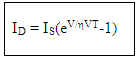 where I D – diode current. (Positive for forward and negative for reverse)
EU S – constant reverse saturation current
V – applied voltage. (Positive for forward and negative for reverse)
 – factor dependent on the nature of the semiconductor. (1 for
germanium and 2 for silicon)
V T – volt equivalent to the temperature given by T/11600. (T is
Temperature in Kelvin)
When a direct voltage is applied across the terminals of a diode, the diode begins to conduct. During conduction, the cut-off or threshold voltage exceeds the applied forward voltage. The threshold voltage for a germanium diode is 0.3V and for a silicon diode it is 0.7V. Direct current (milliampere range) initially increases linearly and then increases exponentially for high currents.
When a reverse voltage is applied, a reverse saturation current flows through the diode. The diode remains in the non-conducting state until the reverse voltage drops below the zener voltage. As the reverse voltage approaches the peak reverse voltage, a breakdown called 'avalanche breakdown' occurs. During decomposition, minority charge carriers ionize stable atoms, which are followed by chain ionization to generate a large number of free charge carriers. Thus, the diode gets short-circuited and gets damaged.
Note: When diodes are connected in series, their equivalent peak inverse voltage increases, while in parallel connection the current carrying capacity increases.
As the temperature increases, the thermally generated electron pairs also increase, thus increasing the conductivity in both directions. The reverse saturation current also increases with increasing temperature. The variation is 11% per °C for a germanium diode and 8% per °C for a silicon diode. On the other hand, the diode current is doubled for every 10°C increase. With increasing voltage, the trigger voltage on the forward characteristics is reduced while the peak reverse voltage increases.
Note: The peak reverse voltage can be reduced by increasing the doping level. The same concept is used to design zener diodes.
Diode resistances: The resistance associated with the diode can be evaluated in three ways and the three types of resistance associated with a diode respectively.
· DC or Static Resistance: It is the relationship between the diode voltage and the diode current at any point on its characteristic curves. It is defined at a point on the characteristic curves.
· AC or dynamic resistance: It is the ratio between the variation in diode voltage and the variation in diode current. It is defined at a point on the characteristic curves on a tangent.
· Average AC resistance: It is the ratio between the variation in diode voltage and the variation in diode current along a straight line that joins two operating limits.
Figure 13: Diode resistance characteristics graph display
Diode Capacitances: Diode exhibits two types of capacitances, transition capacitance and diffusion capacitance.
. Transition capacitance: The capacitance that appears between the positive ion layer in the p region and the negative ion layer in the p region.
· Diffusion capacitance: This capacitance originates due to the diffusion of charge carriers in the opposite regions.
The transition capacitance is very small compared to the diffusion capacitance.
In the reverse bias transition, the capacitance is dominant and is given by:
 where C T – transition capacitance
A – cross-sectional area of the diode
W – width of the depletion region
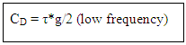
In forward bias, the diffusion capacitance is dominant and is given by:
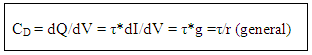 where C D – diffusion capacitance
dQ – change in charge stored in the depletion region
V – change in applied voltage
 – time interval for voltage change
g – diode conductance
r – diode resistance
The diffusion capacitance at low frequencies is given by the formula:
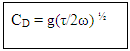
 The diffusion capacitance at high frequencies is inversely proportional to the frequency and is given by the formula:
 Note: The variation of diffusion capacitance with applied voltage is used in the varactor design.
Diode Switching Time: In AC applications, when the diode is switched instantaneously from a conducting state to a non-conducting state, it needs some time to return to the non-conducting state and behaves short-circuited for a small period of time in the reverse direction. This is because when the polarization of the diode is changed suddenly, the majority charge carriers migrated to another region are the minority charge carriers in the region. Specifically, holes are the minority carriers that migrated from p-type to n-type in reverse bias. . These holes require some time to return to the non-conducting state, which is called 'reverse recovery time'. The reverse recovery time is the sum of the storage time and the transition time.
· Storage time: The period of time during which the diode remains in a conducting state even in the reverse direction.
· Transition period: The time taken to return to the non-driving state.
It is desirable that these diodes have minimum switching or reverse recovery time t rr . The switching time of the diodes is on the order of a few nanoseconds to 1 microsecond. Fast-switching diodes with switching times of up to a few picoseconds are now also available.
Figure 14: Graph display of diode switching time characteristics
Identification:
A diode is marked with a bar that indicates the cathode terminal of a diode, as shown in the figure below:
Fig. 15: Image showing the identification of the diode terminals
Note: Various small signal diodes like IN4148, 0A90 and rectifying diodes like IN4001-4007, IN5400-5408, BY125-127 are available with different current, reverse saturation current and peak reverse voltage rating.
Forms
Application:
Diodes are used in diverse applications like rectification, clipper, clamper, voltage multiplier, comparator, sampling ports and filters.
1. Rectification – Rectification means converting AC voltage to DC voltage. Common rectification circuits are half-wave rectifier (HWR), full-wave rectifier (FWR), and bridge rectifier.
· Half wave rectifier: This circuit rectifies the positive or negative pulse from the AC input. The figure is shown below:
Figure 16: Circuit diagram of diode-based half-wave rectifier
· Full wave rectifier: This circuit converts the entire AC signal into DC. The figure is shown below:
Figure 17: Circuit diagram of diode-based full-wave rectifier
· Bridge rectifier: This circuit converts the entire AC signal into DC. The figure is shown below:
Figure 18: Circuit diagram of diode-based bridge rectifier
2. Clipper – The diode can be used to clip some part of the pulse without distorting the remaining part of the waveform. The figure is shown below:
Figure 19: Circuit diagram of diode-based Clipper
3. Clamp – A clamp circuit restricts voltage levels to exceed a limit, changing the DC level. Peak to peak is not affected by fixation. Diodes with resistors and capacitors are used to make clamping circuits. Sometimes independent DC sources can be used to provide additional displacement. The figure is shown below:
Figure 20: Circuit diagram of diode-based clamper
Data Spreadsheet Analysis
Data Spreadsheet Analysis:
Diode datasheets provide valuable information about their various parameters such as:
· Peak reverse voltage,
· Reverse saturation currents at specified reverse voltages,
Maximum direct current,
· Capacitance levels,
longer recovery time,
· Storage and operating temperatures,
· Repetitive direct current spike,
Direct surge current peak,
· Average surge current and more. .
Graphs to represent current voltage characteristics and temperature dependencies are also provided.
Rectifier diodes on the market:
· Diodes designated IN4001 to IN4007 are available with a maximum forward voltage of 1.1 V and 1A being the maximum rectification current. The maximum reverse current is 5 uA and PIV (Peak Reverse Voltage) ranges from 50V to 1000V.
· Another series of diodes is IN5400 to IN5408 with maximum forward voltage of 1.2 V and 3A being the maximum rectification current. The maximum reverse current is 5 uA and PIV (Peak Reverse Voltage) varies from 50V to 1000V.
Testing a diode
Testing a diode:
A diode may be open-circuited or short-circuited when damaged. It can be tested using a multimeter by following the steps below:
1. Insert the test leads into the required sockets: The digital multimeter will have several sockets for the test leads. Insert these probes and check that they are already in the correct sockets. Typically, they are labeled COM for common and the others for current or voltage. It is usually combined with the voltage measurement socket.
2. Turn on the multimeter and select the maximum resistance range.
3. Check resistance in forward and reverse direction. Place the red test lead on the anode of the diode and the black test lead on the cathode to measure direct resistance. Place the red test lead on the cathode of the diode and the black test lead on the anode to measure the reverse resistance. The forward resistance should be very small in the few ohms, while the reverse resistance should be very high in the mega ohm range. If the forward resistance is too high, the diode will be open-circuited and if the reverse resistance is too small, the diode will be short-circuited.
4. Another way is to select the diode on the multimeter. Place the red test lead on the anode of the diode and the black test lead on the cathode and the multimeter beeps, then it indicates a short circuit, otherwise it is open. Place the red test lead on the cathode of the diode and the black test lead on the anode and if the multimeter does not beep then it indicates an open circuit otherwise if it beeps then the diode is shorted.
5. Turn off the multimeter: After the resistance measurement has been made, the multimeter can be turned off to save batteries. It is also advisable to place the function switch in a high voltage range. This way, if the multimeter is used again for another type of reading, no damage will be caused if it is inadvertently used without selecting the correct range and function.