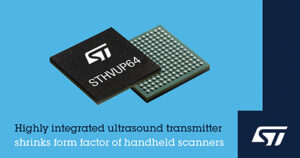
STMicroelectronics has launched a 64-channel ultrasound transmitter with new features to enhance image quality and convenience for high-performance portable medical and industrial instruments.
 Today's ultraportable scanners are about the size of a smartphone, but offer image quality comparable to large, expensive high-end systems from just a few years ago. ST's STHVUP64 transmitter, which drives the instrument's piezoelectric transducers, is driving the next stage in this evolution, adding extra flexibility, digital beam steering and space-saving innovations.
With 64 channels, the STHVUP64 offers a highly integrated solution aimed at the portable wireless scanner segment. It can drive up to 256 probe elements directly, eliminating expensive, high-voltage switches normally required between the transmitter and probe.
Designers can thus reduce the list of materials and take advantage of space savings inside the device.
The STHVUP64 also introduces a new 5-level output capability in addition to the common 3-level output, which increases flexibility for optimizing image quality. The STHVUP64's high current supply, up to ±400mA, allows you to drive the transducers at high speed to enable multiple imaging modes. The high drive force also helps achieve a pulse duration as short as 5ns, which improves control of the transducers to maximize image detail. The transmitter supports continuous wave (CW) and pulsed wave (PW) modes of operation to enable multiple types of analysis, including cavities and liquid flow.
Additionally, digital beam steering improves directional control, allowing for greater precision than conventional analog steering using delay circuits. By integrating the logic on the chip, the transmitter can be used without a companion chip, such as an FPGA dedicated to beam steering. This saves PCB space and routing complexity, and bypasses FPGA design challenges.
Also new is that the transmitter has a self-biased driver architecture that eliminates any need for power supply decoupling capacitors that are normally placed outside the chip. This helps ensure a smaller circuit area as well as reducing the bill of materials (BOM). Additionally, it is housed in a smaller package than comparable alternative ICs, thus providing designers with greater flexibility to create next-generation products in even smaller form factors.
While it has extremely low power consumption, which is critical for battery power delivery systems, the STHVUP64 is feature-rich for a superior user experience. There is on-chip memory to store transmission patterns and synchronization is possible using a clock signal of up to 200 MHz to improve image quality by minimizing jitter. The IC also provides a communications port that supports various CMOS signaling standards as recommended for today's highest system clock signal frequencies.
Built-in protection includes noise blocking, thermal protection, undervoltage protection and current recirculation protection. There is also a diagnostic log that allows direct reading of the causes of interruptions to facilitate debugging in the event of a malfunction.
The transmitter is built using ST's proven BCD8s-SOI technology that supports analog (bipolar), digital (CMOS) and power (DMOS) circuits on the same chip. It's in production now, in a 10mm x 10mm x 1.4mm, 196-ball FC-BGA196 package.

