This project explains how to interface the SD card with an AVR microcontroller . In this project, we use an ATMEGA16 microcontroller. The microcontroller runs on a 5V power supply with an integrated crystal frequency of 8 MHz. A 2 GB SDSC card from Transcend, but the code will work with most SD cards. The SD card is formatted with FAT32. The ultimate goal of this project is to read a file from the FAT32 file system from the SD card.
The SD card was formatted as FAT32 before interfacing. The generalized code for FAT32 is written to interface with the SD card. Explanations about the FAT32 file system and how to access files from this file system are explained in this project.
The following section explains the working of the SD card in detail.
SD CARD
The SD card consists of two basic semiconductor sections, a ' memory core ' and an ' SD card controller '.
The 'memory core' is the region of flash memory where the actual file data is saved. When we format the SD card, a file system will be written to this region. So this is the region where the file system exists.
The 'SD card controller' helps communicate the 'memory core' with external devices like microcontrollers. It can respond to certain sets of standard SD commands and read or write data from the memory core to the external device.

The capacity of the 'memory core' is referred to as the size of the SD card. In addition to the 'memory core', there are certain registers associated with the 'SD card controller'. These records store the status of the SD card. The contents of these records are read-only.
SD card can be connected to microcontroller using serial data bus. It can connect using 'SD bus' or 'SPI bus'. The 'SD bus' is designed for high speed, whereas the SPI bus can only operate at much lower speeds. The microcontroller can read or write data to the memory core and read the registers using standard SD commands sent over these serial buses.

In this project, the memory card interface is done using the SPI bus. Certain commands are not available for SPI interface mode and also the speed will be lower than SD mode. But this type of interface is much simpler, especially due to the fact that most of the microcontroller has an integrated SPI hardware module.
This section summarizes that the SD card has an internal controller chip, a central memory region. The internal controller can decode the commands, provide serial interface while the memory core region is where the file system is implemented.
Based on this knowledge, the following section attempts to explain the concept of the SD card functional layer.
(header = SD Card Functional Layers)
SD CARD FUNCTIONAL LAYERS
The internal part of the SD card can be explained with the help of the functional layer concept. Basically there are three layers
1) Serial Interface Layer
two) SD command layer
3) File system layer

The 'serial interface layer' and the 'SD command layer' can be seen as residing within the 'SD controller' and the 'file system layer' can be found within the 'memory core'. As the ultimate goal of this project is to read a FAT32 file system file from the SD card, it is necessary to access all three layers properly.
1) SERIAL INTERFACE LAYER
This layer provides serial interface of the SD card with the microcontroller. In this project the SPI bus is used for the serial interface. The following diagram shows how to interface more than one SD card with a microcontroller.

In this type of interface the microcontroller is called 'Host' and the SD card is called 'Slave'. The microcontroller initiates all data transfers. The clock is also controlled by the microcontroller. The microcontroller is free to choose between SD cards by activating the respective CS (Chip Select) pin.
Data is transmitted from microcontroller to SD card using MOSI (Master Output Slave Input) channel and data is transferred from SD card to microcontroller using MISO (Master Input Slave Output) channel.
The pinout of an SD card for SPI interface mode is shown in the following figure.


The microcontroller used in this project works on 5V power supply, but the SD card can only support up to 3.3V. The logic levels of 5V and 3.3V are different and can cause problems. A 3.3V logic level device can read the logic 0 of a 5V device as logic 1. Likewise, the 5V logic level device can read both the logic 0 and logic 1 of a device 3.3V logic level as logic 0 only. This problem can be solved by using a bidirectional level converter introduced between the SPI pins of the microcontroller and the SD card.
The circuit diagram for the serial interface of an SD card with the microcontroller including the level converter is shown below.
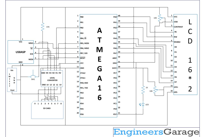
The programmer is 'USBasp' which is also an SPI device. It is connected to the SPI bus along with the SD card. LM1117 is used to supply 3.3V power to the SD card and also to the low voltage side of the level converter. The level converter is a four-channel device with a MOSFET controlling each channel. This type of level converter is suitable for SPI, I2C buses. The image of the level converter used in this project is shown below.


The configured AVR SD card image

(header = SD Command Layer)
two) SD COMMAND LAYER
The SD card only accepts a set of standard SD commands. Using these commands, a microcontroller can read the registers from the SD card and also read/write the 'Memory Core'.
There are six basic registers found on SD cards, details of which are given in the following figure:

All SD commands supported in SPI mode are 6 bytes long. The MSB is transmitted first and the actual command occupies the first byte. The command byte is followed by its 4-byte arguments. The last byte is the CRC byte corresponding to the command and argument bytes.
The structure of a command block in the SPI interface mode of an SD card is shown in the following figure

CRC is only required for some commands in SPI mode. The CRC used is the 7-bit CRC, with a generating polynomial given by
x 7 + x 3 + 1
The CRC calculation is presented below;
G(x) = x 7 +x 3 + 1
M(x) = (initial bit) ? x 39 + (host bit) ? x 38 +…+ (last bit before CRC) ? x 0
CRC (6…0) = Remainder ( (M(x) ? x 7 ) / G(x) )
The 7-bit CRC forms the first seven bits of the last byte of the command and the eighth bit (final bit) must always be set to one.
Using the above equations and the trailing bit condition, the CRC byte for the 0th command and the 8th command are calculated as 0x95 and 0x87 respectively. For all other commands the CRC is ignored by almost all SD cards.
The standard SD commands, their arguments, response type, and description are given in the following figure.


COMMAND RESPONSE
In SPI mode, the SD card responds to all incoming commands using three basic command response types, R1, R2, and R3. Each bit in the response block contains some specific details about the status of the SD card.
Answer – R1

Answer – R2

Answer – R3

The R3 response is only available for the 58th command (READ_OCR).
COMMANDS TO WRITE DATA
Data can be written to the 'Memory Core' of the SD card using the commands below followed by the actual data;
WRITE_BLOCK – Writes data in a single block
WRITE_MULTIPLE_BLOCK – Write data to multiple blocks
WRITE_BLOCK
On SD card, a block is always considered as consecutive memory locations of 512 bytes. Suppose a block from 2000 memory location needs to be written with some data using WRITE_BLOCK command. The command package should look similar to the one shown below;
1 st byte (command) – 0x18
2 and for 5th byte (argument) – 0x000007d0 (Even if there are no arguments for other commands, this field must be set to zero)
6th byte (CRC) – any value
Once the command is sent, the microcontroller should receive the R1 response. All bits in the response must be zero. After receiving the R1 response byte with a zero value, the microcontroller can send the data to be written to the SD card. The length of the data must be 512 bytes, even if the actual data is fewer bytes.
The 512-byte data must be preceded by a data token byte and must end with a 16-bit CRC byte. These 1 + 512 + 2 = 515 bytes form a data packet. The Data Token is a byte with all bits except the LSB set to 1 (0xFE). The data packet format is shown below:

To write the next block of data, the WRITE_BLOCK command must be sent again.
WRITE_MULTIPLE_BLOCK
The WRITE_MULTIPLE_BLOCK command differs from WRITE_BLOCK in such a way that this command needs to be sent only once and the following 512 byte data packets will be written to the consecutive memory blocks.
DATA RESPONSE
For each block of data written, the SD card sends a response byte to the microcontroller. The content of the response byte is given as follows:

(header= Commands for reading data and initializing the card)
COMMANDS FOR READING DATA
Data can be read from the SD card 'Memory Core' using the commands below;
READ_SINGLE_BLOCK – Read data from a single block
READ_MULTIPLE_BLOCK – Read data from multiple blocks
READ_SINGLE_BLOCK
On SD card, a block is always considered as consecutive memory locations of 512 bytes. Suppose a block from the 2000th memory location needs to be read using the READ_SINGLE_BLOCK command. The command package should look similar to the one shown below;
1 st byte (command) – 0x11
2 and for 5th byte (argument) – 0x000007d0 (Even if there are no arguments for other commands, this field must be set to zero)
6th byte (CRC) – any value
Once the command is sent, the microcontroller should receive the R1 response. All bits in the response must be zero. After receiving the zero-valued R1 response byte, the microcontroller can read the data from the SD card. 512 byte data will be sent by the SD card in response to each READ_SINGLE_BLOCK command.
DATA TOKEN
Reading 512-byte data must be preceded by a data token byte and must end with a 16-bit CRC byte. These 1 + 512 + 2 = 515 bytes form a data packet. The Data Token is a byte with all bits except the LSB set to 1 (0xFE). The data packet format is shown below:

If any problem occurs during the reading process, the microcontroller will only receive a single-byte data error token. The data error token bits represent the type of error that occurred. The data error token is shown below:

To read the next data block, the READ_SINGLE_BLOCK command must be sent again.
READ_MULTIPLE_BLOCK
The READ_MULTIPLE_BLOCK command differs from READ_SINGLE_BLOCK in such a way that this command needs to be sent only once and consecutive 512-byte memory locations will be read continuously.
COMMANDS TO INITIALIZE THE MEMORY CARD
Before the memory card can respond to these commands, it must be initialized in SPI mode. Certain commands must be sent one after the other to initialize the SD card. The SD card will be in SD interface mode upon reboot. Therefore, the first command sent to the SD card must include the correct CRC byte.
The steps required to boot SD card into SPI mode using commands are as follows:

Once the SD card is initialized, we can start using the read and write commands. SD command layer commands like READ_SINGLE_BLOCK, READ_MULTIPLE_BLOCK, WRITE_BLOCK etc. are mainly used to interact with the file system layer.
The following section explains the features of the FAT32 file system and shows how data can be read in this file system implementation.
(header = file system layer)
3) FILE SYSTEM LAYER
This section explains the implementation of the SD card FAT32 file system in detail. The FAT32 file system is written to 'Memory Core' when it was formatted. FAT32 stands for File Allocation Table 32, which means it has a 32-bit file allocation table.
All the data in a file is shuffled in the Memory Core and the FAT (File Allocation Table) maintains the location of the next block corresponding to the location of the current block.
SECTORS
The Memory Core has 8-bit (1-byte) memory locations. Consecutive 8-bit memory locations are grouped into 'Sectors'. A FAT32 sector is generally 512 bytes per sector. The grouping of memory bytes to form Sectors is shown in the following figure.
SETS
Consecutive Sectors are grouped together to form 'Clusters'. The number of sectors per cluster depends on the size of the entire file system. The grouping of Sectors to form Clusters is shown in the following figure.
 PACKAGED STORAGE
All data in a file is shuffled into the Memory Core as data clusters. The following figure shows how data from three files called A, B, C are shuffled in Memory Core. FAT (File Allocation Table) maintains the location of the next Cluster corresponding to the current Cluster location of the file.

FAT32 FILE SYSTEM FORMAT
The FAT32 file system is stored or written inside the Memory Core in a specific defined format. There are certain sectors defined at the beginning of the memory core which are followed by clusters. The format of a FAT32 file system is shown below:

The first sector is the MBR (Master Boot Record), which follows a significant number of unused sectors. The unused sectors are followed by the reserved sectors, among which the first sector is the BOOT sector. Reserved Sectors are followed by FAT Sectors. The number of FAT sectors depends on the size of the file system. FAT sectors are followed by some hidden sectors. Hidden Sectors are followed by Clusters.
MBR
The MBR (Master Boot Record) is the first sector of the 'Memory Core' and aims to store information about the partitions within the file system. MBR can contain details of four fundamental partitions. MBR has one sector and the important bytes of MBR are shown below.
Partition information bytes are 16 bytes long and each of them contains important information about the corresponding partitions. The last byte of the MBR is the signature byte which contains a specific value (0xAA55 for FAT32) that can be used to check whether the sector is MBR or not. The first four-byte sector number of the partition can be read from the 8th bit to 11th bit of the partition information bytes, as shown below:

STARTUP SECTOR
The boot sector is the first sector within a partition. This sector contains all the valuable details about the file system within that particular partition.

The first two bytes are Check Bytes which together contain a specific value, usually 0xE9 or 0xEB. The 11th and 12th bytes when read together give the number of bytes per sector for the file system. FAT32 generally has 512 bytes per sector. The 13th byte contains the number of sectors per cluster for the file system. The 14th and 15th bytes together read the number of reserved sectors before the FATs, starting at the beginning of the partition. The 16th bit contains the value of the number of FATs in the file system. The 4 bytes from the 27th byte to 30th byte can be read together to get the number of hidden sectors between the FATs and the first cluster of the partition. The 4 bytes from the 43rd byte to 46th byte contain the address of the root cluster, which is the first cluster of the partition (usually 2). The 47th and 48th bytes can be read together to obtain the location of the sector where the file information is stored (directory sector).
FS INFORMATION SECTOR
The Sector number of the FS Info Sector is obtained from the 47th and 48th byte of the boot sector. It contains the current status of the Clusters. It can contain the value of the total number of currently free clusters and also the cluster number of the next free cluster within the file system, as shown below:
FS DIRECTORY SECTOR
It is the first sector within the first file system cluster. The first Cluster always starts with Cluster number 2. It is also the first Data Sector of the partition. The FS Directory is 32 bytes and therefore there are 16 FS Directories per FS Directory Sector. The sector number of the first sector of the FS directory can be found using the following equation:
DIR_SECTOR_NUM = NO. OF RESERVED SECTORS + NO. OF FAT + NO. OF HIDDEN SECTORS
Each FS directory contains significant details about a single file, as shown in the following figure:

The first 11 bytes contain the file name and the 11th byte contains the file attribute. The byte attribute is used to verify a valid file. The byte content of the attribute is shown in the following figure:

The 20th and 21st bytes together hold the upper bytes of the file's first cluster number while the 26th and 27th bytes contain the lower bytes of the file's first cluster number. The last four bytes contain the file size.
THE LOGIC FOR READING A FILE FROM THE FAT32 FILE SYSTEM
A file with a specific name can be read from the FAT32 formatted file system using the logic shown below; Take a closer look and you will see that the entire process finally ends with a Sector reading. This SD card memory core sector read can be obtained using the READ_SINGLE_BLOCK command from the SD command layer only.

(header= Using FAT32)
USING FAT32 (FILE ALLOCATION TABLE 32)
FAT32 are sectors in which every 32 consecutive bits together contain the number of clusters. Simply every 32 bits points to a specific cluster. Since a Cluster is typically 512 bytes, there will be 128 Cluster pointers within the Sector. This forms the 32 FAT32 File Allocation Table.
The next Cluster pointer number within FAT32 corresponding to a current Cluster number can be calculated using the following equation
FAT SECTOR NUMBER FOR NEXT CLUSTER POINTER = FIRST SECTOR NUMBER OF PARTITION
+ NUMBER OF RESERVED SECTORS
+ ((CURRENT CLUSTER NUMBER * 4)
/BYTES PER SECTOR)
The following figure shows the method of reading a file that has been scrambled on 'Memory Core' flash using FAT32.

Yellow indicates Clusters that have the specific file data and corresponding Cluster pointers within FAT32. The red lines indicate finding the next Cluster pointer corresponding to the current Cluster and the green line indicates finding the next Cluster using the Cluster number stored within the FAT32 Cluster pointers.
THE CODING DETAILS
As there are three functional layers namely serial interface layer, SD command layer and file system layer, coding is also done for each of the layers separately and then combined. The code layers are shown in the following figure:

The microcontroller reads and writes data using the file system layer. The file system layer interacts with the SD command layer using only the READ_SINGLE_BLOCK command. The SD command layer interacts with the serial interface layer using SPI transmit and SPI receive function calls. The entire microcontroller system interacts with the SD card using the SPI bus interface.
Function pointers have been used for effective interaction between different layers. Structures and dynamic memory allocation were used to store and access 512 bytes of data at a time.


