The circuit presented here in this project generates two different types of waveforms using two OP-AMP LM741 chips. Generates square wave and triangle wave. These waveforms can be applied as input to any other circuit to test its operation. As square wave can be applied to any digital device as pulse input and triangle wave can be given to sweep frequency generator which will generate different frequencies (minimum to maximum frequency sweep) as per the positive ramp (or negative) of the triangle wave is applied.
The circuit is built using two LM741 operational amplifier chips . The first LM741 is used to generate square wave and the second will generate triangular.
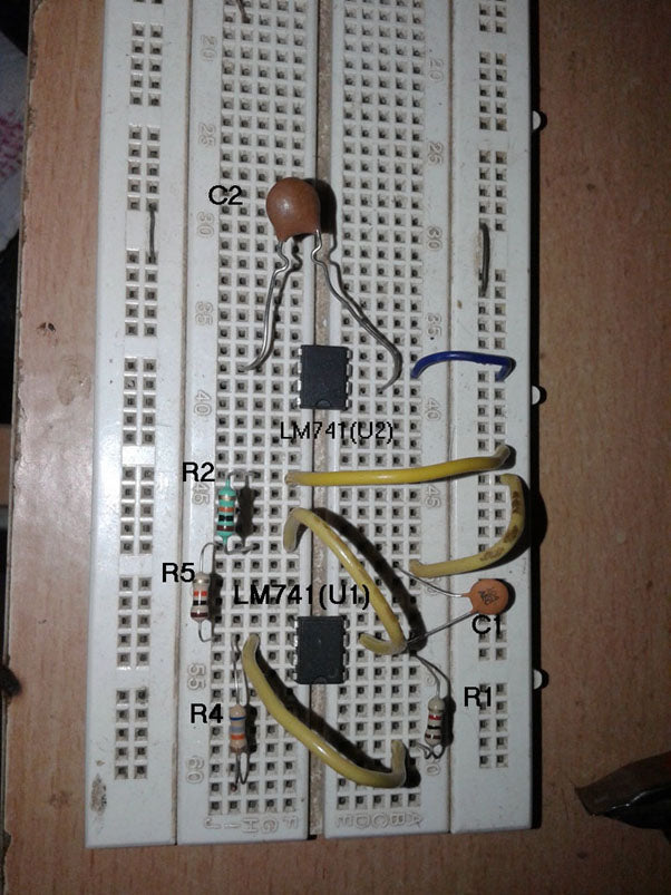
In 1 st LM741 at the inverting terminal, the output feedback is given through the resistor R1 and the capacitor C2, while at the non-inverting terminal the feedback is given by the voltage divider of R2 and R5. The output of this is given directly to the inverting terminal 2 and LM741 to R4. 2 and LM741 together with R4 and C1 form an integrator circuit. Its non-inverting terminal is grounded. Both op amps receive +Vcc and –Vee supplies to respective pins 7 and 4 as shown.
Here is the photograph of the circuit built on breadboard

Fig. 1: Waveform generator prototype using LM741 circuit on breadboard
Circuit Operation
· Suppose that initially the output of U1 is +Vcc
· Then capacitor C2 will start charging through R1
· When the capacitor voltage increases to more than the voltage at the non-inverting terminal given by the equation
V1 = (R2 / (R2+R5))× Vo = (10/20)× Vo = 0.5× Vo
· The output of U1 becomes –Vee
· Then the capacitor starts discharging through R1
· Again, when the capacitor voltage decreases to less than the voltage given by the same equation above, the output becomes +Vcc again
· Thus the cycle repeats itself and produces a square wave output with a period of time determined by the RC components R1 and C2
This square wave output is provided as input to an integrator circuit
· The integrator converts square wave into triangle wave
· When the output of U1 is +Vcc, the capacitor C1 charges to the maximum value and provides a positive ramp at the output of U2
· And when the output U1 is –Vee, the capacitor C1 discharges and generates a negative ramp at the output of U2
· This way we obtain a triangular wave as the output of U2
Here is the photograph of the final output of the circuit in DSO

Fig. 2: Image showing the final output of the circuit in the DSO
Note: – the circuit will produce a perfect triangle wave output only for certain frequency values. Because the integrator also works as a low-pass filter. Therefore, for very low frequencies the output will be clipped (because of high gain) and at high frequencies the output will be very low (because of low gain).
Circuit diagrams
| circuit_27 |  |
Project Components
- Capacitor
- Resistor


