In previous projects, the power source used was the AC mains. In this project, solar energy will be harnessed through a solar panel and will be regulated to charge a 3.7 V battery. The 15 Watt solar panel used in the circuit has a DC output voltage of approximately 22 V. The DC output of the solar panel is not regulated and needs to be ripple-free using a voltage regulator. Once the voltage taken from the solar panel is regulated to desired levels, it can be used to power charging circuits. In the project, the regulated voltage is used to charge a battery.
The project involves shunting DC voltage from the solar panel, regulating input voltage, adjusting voltage and protecting against current. IC LM-317 is used for voltage regulation while a variable resistor is used to set the output voltage to desired levels. The output voltage of the LM-317 voltage regulator can be between 1.25V and 37V, which is adjusted to 4.2V, which is suitable for charging a 3.7V battery.
Required components –

Fig. 1: List of components required for regulated solar energy supply
Circuit Connections –
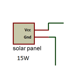
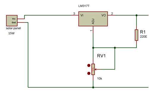
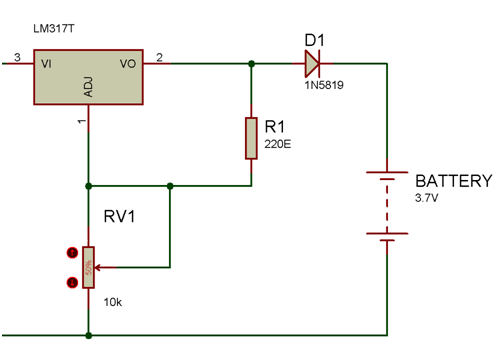
The 15 watt solar panel has two VCC and ground terminals that serve as indicated by their names. The VCC terminal of the panel is connected to the voltage input terminal of IC LM-317 and the ground terminal is connected to a common ground. A variable resistor is connected to the adjustment pin of the LM-317 and a 220 ohm programming resistor R1 is connected to the voltage output pin of the regulator IC. A diode D1 with its anode connected to the voltage output terminal of the IC regulator is connected in series to one of the output terminals of the circuit. The LM-317 voltage output terminal and common ground serve as output terminals. A 3.7V battery is connected to the output terminals for charging.
How the circuit works –
The working of the circuit can be divided into the following operations –
1. Extracting DC voltage from the solar panel
2. Voltage regulation
3. Voltage adjustment
4. Reverse current protection
Extracting DC Voltage from Solar Panel
The solar panel is used to convert solar energy into electrical energy. The phenomenon of converting solar energy into electrical energy is called the photovoltaic effect. This effect generates voltage and current at the output on exposure to solar energy. A 15 Watt, 22 Volt solar panel is used in the project. The panel has a voltage drop of 2 to 2.75 V and a maximum current output of 681 mA. The energy harnessed from the panel will be used to charge a 3.7 V 1000 mAHr battery. A solar panel consists of several solar cells or photovoltaic diodes. These solar cells are PN junction diodes and can generate an electrical signal in the presence of sunlight. When exposed to sunlight, this solar panel generates a DC voltage output of 21 to 22 V at its terminals.

Fig. 2: Solar Panel Circuit Diagram
Voltage regulation
The output voltage of the solar panel is about 22V. it needs to be set to a lower value to charge the battery. The 3.7 V battery requires a voltage of 4.2 V for proper charging. LM317 voltage regulator is used to regulate the voltage output of the solar panel.
LM317 is a monolithic positive voltage regulator IC. As it is monolithic, all components are built into the same semiconductor chip, making the IC small, with lower power consumption and low cost. The IC has three pins – 1) Input pin where maximum 40 V DC can be supplied, 2) Output pin which provides an output voltage in the range of 1.25 V to 37 V and 3) Tuning pin which is used to vary the output voltage corresponding to the applied input voltage. For an input of up to 40 V, the output can vary from 1.25 V to 37 V.
There is an OPAM (operational amplifier) built into the IC whose inverting input is connected to the tuning pin. The non-inverting input is defined by a bandgap voltage reference whose voltage is independent of temperature, power supply, and circuit load. Therefore, the LM317 provides a stable reference voltage of 1.25V at its tuning pin. The reference voltage of 317 can be from 1.2V to 1.3V. The output voltage of 317 can be adjusted within a defined range using a resistor divider circuit between the output and ground.
To set the desired voltage at the output of the LM317, a resistive voltage divider circuit is used between the output pin and ground. By the effect of this setting, the voltage at the output pin can be adjusted. The value of the resistive voltage divider needs to be chosen in such a way that it can provide the required voltage range at the output. The voltage divider circuit has a programming resistor which has one fixed resistance (shown as R1 in the schematics) and another is a variable resistor (shown as RV1 in the schematics). By setting a perfect relationship between the feedback resistor (fixed resistor) and the variable resistor, the desired output voltage corresponding to the input voltage can be obtained.
For best performance of the IC, the fixed or programmable resistor R1 should be connected as close as possible to the regulator IC so that there is less line drop or noise at the output. RV1 must be connected close to load ground for ground detection and to improve regulation.
The LM317 has the following tolerable power dissipation internally –
Pout = (Maximum IC operating temperature)/ (Thermal Resistance, Junction-Environment + Thermal Resistance, Junction-Enclosure)
Pout = (150) / (65+5) (values according to technical data sheet)
Pout = 2W
Therefore, the LM317 can internally sustain a power dissipation of up to 2 W. Above 2 W, the IC will not tolerate the amount of heat generated and will start to burn. This can also cause a serious fire hazard. Therefore, a heat sink is required to dissipate excessive heat from the IC.

Fig. 3: Circuit diagram of IC based voltage regulator LM317 for solar power source
Voltage adjustment
To charge the 3.7V Li-ion battery an input voltage of 4.2V is required. Therefore, to set the output voltage 317 to 4.7V, RV1 must be set to the required position. Varying the output voltage RV1 between 1.1V and 10.4V can be obtained.
Back current protection
When there is no sun rays around, the solar panel has no voltage. At the output terminals, the battery still has some voltage, which causes the output voltage to exceed the input voltage (solar panel voltage). Therefore, there is a reverse flow of current from the output to the input side and the battery starts discharging through the regulator IC 317 causing damage to it. By using a diode at the output, the reverse flow of current from the output terminal (battery) to the input terminal (solar panel) through 317 can be avoided, thus keeping the voltage regulator IC safe.

Fig. 4: Countercurrent protection circuit diagram
Tests and precautions –
The following precautions must be taken while assembling the circuit –
• To drive high load current at the output, the heat sink must be mounted in the regulator holes. This will prevent the regulator IC from exploding. The 317 IC can internally handle power dissipation of only up to 2W.
• The drop voltage of IC LM317 is about 1.5V to 2.5V depending on the output current. Therefore, the input voltage must be 1.5V to 2.5V greater than the desired output voltage.
• A diode (shown as D1 in the schematics) that receives less drop must be used so as not to reduce the output voltage. This is why the 1N5819 diode is used, which suffers fewer drops.
• To drive high loads, a high power solar panel must be used.
Once the circuit is assembled, measure the voltage and current readings using a multimeter. To charge a 3.7 V battery, a voltage of 4.2 V is best suited. The maximum current supplied by the solar panel is given by –
Imax = Solar panel power/Solar panel voltage
Imax = 15/22
Imax = 681mA
With this current, the time required to charge the battery will be as follows –
Time required to charge, T = 1Ah/0.681A = 1.46 hours (approximately)
The current of the 3.7V battery is 2mA. The current consumed by the battery depends on the charging status. It consumes less current when fully charged.
As the input voltage of the solar panel is 22V and the output voltage of the 317 regulator is 4.2V, the power dissipation across the regulator IC is derived as follows –
Preg = (Vin – Vout)*Ibatt
Preg = (22 – 4.2)*0.002
Preg = 35.6mW
Although the power dissipation of the regulator IC is less than the internally tolerable limit of 2 Watts, it is still recommended to use a heatsink to help cool the regulator IC and increase its lifespan.
The regulated solar power source designed in this project provides regulated and adjustable voltage from 1.1V to 10.4V by varying potentiometer RV1. Therefore, any battery or charging circuit that needs a voltage between 1.1V and 10.4V can draw power from this circuit. As this solar power source provides a maximum current of 681mA, any battery or circuit that uses a maximum current of 681mA can be connected to it.
Circuit diagrams
| Circuit Diagram Regulated Solar Power Supply |  |
Project video

