
There has never been such extensive use of batteries before. Portable electronic devices are becoming increasingly popular and they all run on batteries. With the use of batteries, overcharging and overdischarging are common problems. To avoid excessive charging and discharging of batteries, it is necessary to monitor the charge level of the connected battery. A circuit used for this purpose is called a battery level indicator. A battery level indicator provides indication of the battery's charge or discharge status.
Secondly, some batteries have a high tolerance limit for overcharging and some may explode after a certain charge threshold. That's why it's important to disconnect the battery from charging when it reaches its maximum limit. A battery level indicator provides a visual indication of the battery's status and allows you to disconnect the battery before overcharging it. Furthermore, the battery level indicator encourages the user to charge the battery before it runs out.
Depending on the state of the battery, there are two ways to indicate the charge level: one is the state of charge (SOC) method and another is the death on discharge (DOD) method. SOC is the measure of the charge stored in the battery and DOD is the measure of the degree to which the battery is being depleted relative to the battery's total capacity.
In this project, a battery level indicator is designed using state of charge method. The SOC method is more convenient to use and easier to design. The SOC of the battery can be determined by the voltage level at the battery terminals or by measuring the current output of the battery. In this project, the SOC of a battery is determined by sensing the terminal voltage level of the battery. Therefore, to detect the voltage level of the battery, an integrated circuit is required that can accurately detect the voltage at the battery terminals.
In this design, two lithium-ion batteries are connected in series. Each lithium-ion battery has a nominal voltage of 3.7 V and a maximum charge voltage of 4.2 V and an end-of-discharge voltage of 3 V. The end-of-discharge voltage is the voltage below which any device connected to battery will stop working. To detect the terminal voltage level of battery series, IC LM3914 is used. LM3914 is a bar display driver that can detect the magnitude of analog voltage and indicate the voltage level by lighting up to 10 LEDs. Thus, the IC is designed to indicate ten voltage levels relative to a common voltage reference. The internal 10-step divider is floating and can be referenced to a wide range of voltages.
For voltage indication, LEDs or bar display can be connected to the IC. The IC is capable of interfacing even with 100-step displays. The IC's internal voltage reference can be set from 1.2V to 12V. The IC can allow output current consumption via an LED or bar display from 2mA to 30mA.
In this project, 10 LEDs are interconnected to the IC to indicate the voltage level from 6.2V to 8.45V. As there are 10 LEDs, each LED will indicate an increase of 0.24V in the terminal voltage of the battery series and each LED will consume maximum current of 2mA.
Required components

Fig. 1: List of components required for IC LM3914 based battery level indicator
Circuit Connections
To design this battery level indicator, it is important to understand the pin diagram and pin configuration of IC LM3914. This IC is the main component of the circuit. LM3914 is a monolithic integrated circuit (all components incorporated on a single chip) that senses voltage and can drive 10 LEDs. The LEDs display the voltage level in the form of a bar or dot graph. In bar graph form, the LEDs light up incrementally and continuously, but in dot form, only one LED lights up for the corresponding voltage level. For example, in bar display, when the battery voltage is at 6.7V, three LEDs will light up, but in dot mode, only the third LED will light up.
The LM3914 has 18 pins with the following pin configuration –

Fig. 2: Table listing the pin configuration of the IC LM3914
The LED current is regulated by the IC itself, which eliminates the need for a resistor with the LED. Hence, the IC is powered with a minimum of 3V and the maximum supply voltage can be up to 25V. Do not supply input voltage beyond the maximum rating of the IC. The input signal overvoltage of the LM3914 is +/- 35 V according to the datasheet, but for safety, it is recommended to provide input voltage up to 25 V.
The output current that can be supplied by the LM317 is 2 mA to 30 mA. Internally this IC has a high input impedance buffer and ten comparators (as shown in the internal circuit of the 3914). The buffer operates the signal from ground to the input voltage and is protected against reverse signal and overvoltage. For this protection, a diode is used internally in the input buffer (as shown in the circuit diagram). The function of the buffer is to provide the signal to comparators that are connected in series. Each comparator is biased by a different resistor and these comparators detect different input supply voltages. Then this voltage is indicated by the LEDs at the output (as shown in the circuit diagram).

Fig. 3: LM3914 internal circuit
First of all, the input supply voltage for output indication needs to be defined. For this purpose pin 5 should be used. Pin 5 is a signal pin which is used to detect the analog signal and the level of the same signal is indicated through the LEDs. In this experiment, pin 5 is connected to resistors R4 and R5 (as shown in the circuit diagram). Both resistors have the same value and form a voltage divider network. This network supplies half of the input supply voltage to the signal pin. For example, if the supply voltage is 6V, the signal pin will detect 3V due to the voltage divider circuit.
Secondly, the low to high voltage range and output current need to be defined. For this purpose, the following pins are provided in the LM3914 IC – RHI (pin 6) – To set the highest threshold voltage level
– RLO (pin 4) – To set the lower limit voltage level
– REF adjustment (pin 8) – To set the required reference voltage
– REF Out (pin 7) – Determines the brightness of the output LED
To control the brightness of the output LEDs, the current drawn at pin 7 needs to be set. The current drawn by the output LEDs depends on the current drawn at the reference voltage pin (pin 7). About 10 times this current is consumed by each LED, regardless of changes in input voltage and temperature. The current that each LED consumes can also be adjusted using the following equation –
I LED = 12.5/Req (approx.) (from datasheet)
The RLO and RHI pins decide the output voltage range from low to high. The LM3914 indicates the output voltage via LED only in the low to high voltage range.
The REF tuning pin provides the reference voltage to set the desired output voltage range. Internally, the IC has a constant reference voltage of 1.25 V at Ref Out (pin 7) and Ref Adj (pin 8). This reference voltage can be adjusted from 1.25V to 12V. In this experiment, the reference voltage is kept unchanged, so it is 1.25 V.
According to the basic configuration of LM3914, the lowest voltage level is 0V as the RLO and REF ADJ pin is directly connected to ground. But since the RLO and REF ADJ pins are floating, the lowest voltage level can be changed from 0V to the desired voltage level. This is called scale expansion.
In this experiment, the lower voltage level must start at 6 V and the upper voltage must be 8.4 V. For this, some resistors on the REF ADJ and REF OUT pins must be connected so that they can provide the voltage range as per the need.
")
Fig. 4: Circuit diagram showing the basic configuration of the LM3914 with internal circuitry (Source – LM3914 TI datasheet)
To set the desired voltage range, the resistors need to be connected in such a way that they can supply 6V at the RLO pin and 8.4V at the RHI pin. But SIG pin 5 will detect 3V when the supply voltage is 6V. So instead of setting 6V on the RLO pin, it should be set to 3V. Similarly, instead of 8.4V, the RHI pin should be set to 4.2V.
In this experiment, resistors R1 and R2 are connected to provide the required voltages. R2 supplies 3V to RLO pin and RHI pin gets 4.2V. Resistor R1 decides the LED output current.

Fig. 5: Circuit diagram of voltage divider network on RHI and RLO pins
The value of resistances R1 and R2 can be calculated as follows. Resistor R1 determines the LED current.
To calculate R1, the following equations from the datasheet need to be considered –
LED = 12.5/Req
Req = 12.5/I LED
Then,
I LED = current consumed by each LED
As the LM3914 has a minimum output current of 2mA, we will take a minimum current of 2mA so that the LEDs at the output do not consume more battery power.
Each LED current, I LED = 2mA
Req = equivalent resistance
As can be seen from the internal circuit, resistor R1 is in parallel with a series of resistors or resistor divider network that is connected to each comparator. Therefore, the Req in the above equation is the equivalent value of the network R1 and the resistor divider in parallel.
Therefore, to find the exact value of R1, the value of Req must be found –
Required = 12.5/0.002
Req = 6250 ohms
Now to calculate R1 using the following equation
Equivalent resistance, 1/Req = R1 Rdiv (resistor divider network)
According to the internal circuit, the value of a resistor string or resistor divider network is 10k, but according to the 3914 datasheet, the typical value of this resistor divider is 12k.
So Rdiv = 12k
Req = 6250 ohms
1/Req = 1/R1 + 1/ Rdiv
1/R1 = 1/Req – 1/ Rdiv
1/R1 = 1/6250 – 1/12000
R1 = 13k (approx.)
The lowest voltage level needs to be set by resistor R2. Now to calculate the voltage divider circuit R2 on the pin needs to be considered. For proper calculation of resistor R2, consider the circuit shown below –

Fig. 6: Circuit diagram showing calculation of resistances for voltage divider network at RLO and RHI pins
R2 can be calculated by the following equation –
R2 = VR2 (voltage in R2)/ IR2 (current in R2)
Calculation of current in R2, IR2
From the above figure of voltage divider network, it is clear that
IR2 = IR1 + Iadj
Now,
Iadj = Current flowing out of reference adjustment pin
According to the datasheet, the minimum tuning pin current is 75uA, so to decrease the error term, let's consider 75 uA as Iadj.
As the IC has internal constant reference voltage of 1.25V at Ref Out (pin 7) and Ref Adj (pin 8). Therefore, a constant current will flow through R1.
Current in R1, IR1 = Vref(reference voltage)/ R1
IR1= 1.25/6250
IR1 = 200ua
Now, putting the values of IR1 and Iadj, we can calculate IR2
IR2= 200 + 75 (both in uA)
IR2 = 275ua
Now in the calculation of R2
R2 = VR2 (voltage in R2)/ IR2 (current in R2)
Since R2 will supply 3V to the RLO pin, so VR2 = 3V
R2 = 3/0.000275
R2 = 11k (approx.)
Note that resistor R1 will supply 3V to the RLO pin.
To set a higher voltage level at 8.4V, the RHI pin must get 4.2V. Therefore,
Total voltage drop across RHI = VR1 + VR2
As the voltage drops across R1, VR1 = 1.25V (as REF adj and REF out pin provide a constant reference voltage of 1.25V as explained above)
The voltage drop across R2, VR2 = 3V
Total voltage drop across RHI = 1.25 + 3
Total voltage drop across RHI = 4.25V
Therefore, taking R1 as 13 kΩ and R2 as 11 kΩ, the battery voltage from 6V to about 8.4 V can be detected with a maximum current of 2mA at the output.
In the third step, indication mode needs to be set. There are two types of display for visual indication at the output and these two displays can be configured by the mode selection pin (pin 9). This pin controls the display of the output LEDs. To select Dot mode, pin 9 needs to be floated or open and to select bar graph mode, pin 9 needs to be connected to input power (V+). In this experiment, pin 9 is connected to a switch to change the value of the 9th pin to V+ or float as desired.
Finally, the battery must be connected to IC LM3914. The battery must be connected between pins 2 and 3 of the IC. Pin 3 or V+ pin provides the input voltage of IC LM3914. The positive terminal of the battery must be connected to this pin. Pin 2 or V pin provides ground to the IC and needs to be connected to the negative terminal of the battery.
It is recommended to use a 2.2 uF tantalum and 10 uF aluminum electrolytic capacitor on the ground pin (pin 2) of the LM3914 if the LED wires are 6 inches or longer. This is because long wires increase resistance and inductance and generate input noise.
How the circuit works

Fig. 7: IC LM3914 based battery level indicator prototype designed on a breadboard
All circuit functionality is managed by IC LM3914. The IC is designed to operate as a battery level indicator. Only the additional components like resistors and battery should be connected to the IC.
Testing the Circuit
Theoretically, LED D1 should light up when the battery voltage is 6V and LED D10 should light up when the battery voltage is 8.4V. When measuring the battery terminal voltage with a multimeter, the LEDs light up as follows –
Practical observation table in bar graph display

Fig. 8: Table showing battery level indicator bar graph display
When calculating the error percentage,
Error % = (practical observation – theoretical observation)*100/
Practical observation
Error at lowest voltage level, % error = ((6.2 – 6)*100)/6
Error% = 3.3%
Error at higher voltage level, Error %= ((8.45 – 8.4)*100)/8.4
% error = 0.6%
Therefore, there is a tolerable error observed during the operation of the IC.
Circuit diagrams
| Circuit Diagram-LM3914-IC-Battery Level Indicator | 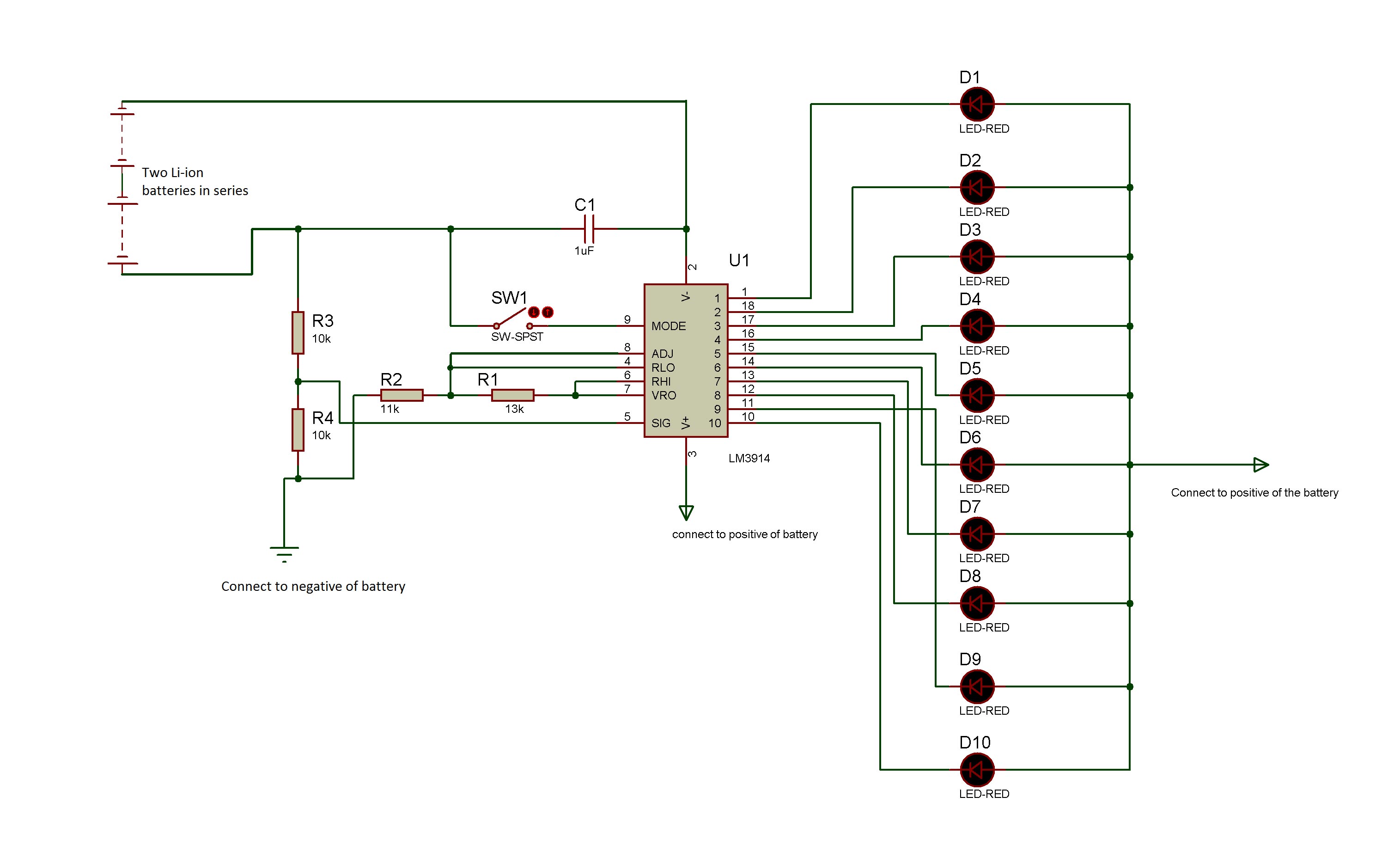 |


