In this article, we embark on an exciting journey to explore the profound impact of transistors on technology. We will delve into the origins of this remarkable invention, tracing its humble beginnings and groundbreaking advancements. From the pioneering work of Bell Labs to the collaborative efforts of brilliant minds, we'll discover the story behind the rise of the transistor.
transistor
It is one of the most important semiconductor components. It was invented by William Shockey in 1947. The term transistor is derived from the abbreviation of the word “transfer resistor”.
Current transfer occurs from a low-resistance circuit to a high-resistance circuit. Transistor revolutionized electronics and led to other inventions such as integrated circuits (IC), optoelectronic devices and microprocessors. Transistors have replaced vacuum tubes in almost all applications.
-
PN connection with forward and reverse bias
The basic function of a transistor is to amplify a weak signal in analog circuits. It is also used as a switch or gate in a digital circuit.
Bipolar Junction Transistor
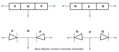
A transistor is an electronic switching device consisting of two PN junctions formed by placing P-type or N-type semiconductors between a pair of opposing layers.
-
Junction transistor is a three-layer (terminal) semiconductor device consisting of two P-type and one N-type regions or two N-type and one P-type regions. These formations are called PNP transistors or NPN transistors.
-
Therefore, there are two types of junction transistors. The emitter and base PN regions come from the diode, while the collector and base PN regions come from the collector diode.
-
In general, the transistor can be viewed as two consecutive PN junctions connected in series as shown in the figure. The middle section, a very thin layer called the base, is the most important area for a transistor to function.
-
The abbreviation BJT (Bipolar Junction Transistor) is often used for this three-terminal device. The term bipolar highlights the fact that holes and electrons are involved in the flow of current.
Transistor Connections
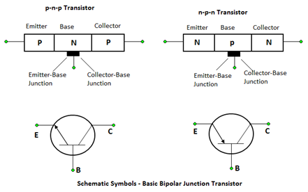
A transistor has three doped areas: emitter, base and collector. All of these areas have connections.
-
Kirchhoff's voltage law and Kirchhoff's current law
Issuer
The left region of the transistor shown in the figure is called the emitter and is more heavily doped than the other two regions of a transistor.
Its main function is to deliver the majority of carriers, whether electrons or holes, to the base. The emitter is always directly polarized with respect to the base, so it can provide many majority carriers.
base
The narrow central region of the transistor is called the base. This area is very thin and slightly doped. The base-emitter connection is forward biased and provides low resistance to the emitter current.
collector
The right part of the transistor, as shown in the figure, is called the collector. He is moderately endowed. The collector region is always inversely polarized with respect to the base. The collector region is physically larger than the emitter region because it does not dissipate much more energy.
-
Zener diode and its properties
The connection between the emitter and base regions is called the emitter-base connection. The connection between the collector and base areas is called the collector-base connection. The circuit symbol of PNP and NPN transistors is shown in the figure.
The arrow in the transistor circuit symbol indicates the direction of conventional current flow and can be used to distinguish an NPN transistor from a PNP transistor. It is shown on the emitter connection.