In the previous tutorial – More Combinational Circuits , the basic concepts of encoder, decoder, multiplexer and demultiplexer were discussed. An encoder is used to encode digital information according to a predefined code system (such as BCD, Gray, etc.). An encoder inputs data (such as from a keypad or keypad) representing familiar numbers, characters, or symbols and generates encoded binary numbers. Thus, it inputs the alphabetic characters and decimal numbers from an input device via individual wires and produces the outputs as binary coded representation of the input symbols.
In communication systems, encoders are used to transmit digital information. There, encoders reduce the number of bits needed to represent digital information, so that the transmission link can transfer the encoded information using fewer lines. Encoders are also used to encode data that will be stored for later use as they facilitate the storage of fewer bits in the available space.
Decoders perform the inverse operation of encoders. They are used to decode binary codes into respective minterms which in turn represent individual symbols and characters. Both encoder and decoder are combinational circuits as their output depends only on the current values of the input.
In this tutorial, the encoder and decoder circuits will be built using 7400 series ICs. From the previous tutorial, it should be known that a decoder can be built using NOT and AND gates. In this tutorial, a 2 to 4 line decoder will be built using 7404 IC for NOT gates and 7411 IC for AND gates. Similarly, an encoder can be constructed using OR gates, AND gates and NOT gates. Here a 4 to 2 line encoder is constructed using 7404 IC for NOT gate, 7408 IC for AND gate and 7432 IC for OR gate.
Required components –

Fig. 1: List of components used to make the SN-7400 series IC-based encoder and decoder
Circuit Diagrams –
The 2 to 4 line decoder has the following circuit diagram –

Fig. 2: Circuit diagram of 2 to 4 line decoder
The 4 to 2 line encoder has the following circuit diagram –

Fig. 3: Circuit diagram of 4 to 2 line encoder
Circuit Connections –
Both decoder and encoder are combinational circuits. Its output depends only on the current value of the inputs. Each circuit has a unique truth table from which the respective Boolean expression for each output can be derived. The minimized Boolean expression is then converted into a logic gate diagram which is built on a breadboard using 7400 series ICs.
The following logic gate ICs are used in constructing the circuits –
7411 IC – The 7411 IC is a 3-input triple AND gate IC. The IC has the following pin configuration –

Fig. 4: Table listing the pin configuration of the 7411 IC
The IC has the following pin diagram –

Fig. 5: Pin Diagram of 7411 IC
The IC requires a supply voltage of 5V which can be tolerated up to 5.25V. The voltage at the AND gate inputs should be 2V for logic high and 0V for logic low. The output of the AND gates has a voltage of 3.4 V for logic high and up to 0.8 V for logic low. The IC operates on a positive logic system. The propagation delay during transit from LOW to HIGH at the output varies between 4 to 18 ns, while the propagation delay during transit from HIGH to LOW at the output varies between 3 to 18 ns.
7408 IC – The 7408 IC has 2-input quadruple AND gates. The IC has the following pin configuration –

Fig. 6: Table listing the pin configuration of the 7408 IC
The IC has the following pin diagram –

Fig. 7: Pin diagram of 7408 IC
The IC requires a supply voltage of 5V which can be tolerated up to 7V. The voltage at the AND gate inputs must be 2V for logic high and 0V for logic low. The output of the AND gates has a voltage of 3.4 V for logic high and 0.2 V for logic low. The IC operates on a positive logic system. The propagation delay during transit from LOW to HIGH at the output is 27 ns, while the propagation delay during transit from HIGH to LOW at the output is 19 ns.
7432 IC – The 7432 IC has 2-input quadruple OR gates. The IC has the following pin configuration –

Fig. 8: Table listing the pin configuration of the 7432 IC
The IC has the following pin diagram –

Fig. 9: Pin diagram of 7432 IC
The IC requires a supply voltage of 5V which can be tolerated up to 7V. The voltage at the inputs of the OR gates must be 2V for logic high and 0V for logic low. The output of the OR gates has a voltage of 3.4 V for logic high and 0.35 V for logic low. The IC operates on a positive logic system. The propagation delay during transit from LOW to HIGH at the output is 3 to 15 ns, while the propagation delay during transit from HIGH to LOW at the output is also 3 to 15 ns.
7404 IC – The 7404 IC has six inverter ports. The IC has the following pin configuration –

Fig. 10: Table listing the pin configuration of the 7404 IC
The IC has the following pin diagram –

Fig. 11: Pin Diagram of 7404 IC
The IC requires a supply voltage of 5V which can be tolerated up to 7V. The voltage at the inputs of the NOT gates must be 2 V for logic high and 0.8 V for logic low. The output of the NOT gates has a voltage of 3.4 V for logic high and 0.2 V for logic low. The IC operates on a positive logic system. The propagation delay during transit from LOW to HIGH at the output is 22 ns, while the propagation delay during transit from HIGH to LOW at the output is 15 ns.
It should be noted that the selected ICs have compatible input, output and power voltage levels as they are taken from a common family (74XX series) of digital ICs.
How the circuit works –
To build the 2-to-4-line decoder and the 4-to-2-line encoder circuit, firstly, their truth table must be known. From the truth table, Boolean expressions for each line of output can be derived. Boolean expression relates the output variables with the input variables by the respective Boolean equation. The derived Boolean equations can be realized by interconnecting logic gates accordingly. The encoder and decoder circuits are constructed as follows –
4 to 2 Line Encoder – An encoder is a digital circuit that performs the reverse operation of a decoder. An encoder has 2 n input lines and n output lines. In the encoder, the output lines generate the binary code corresponding to the input value. In a 4 to 2 line encoder, there are four inputs that represent any four symbols or characters and two outputs that generate the corresponding binary code. In an encoder circuit, it is assumed that only one input is passed at a time, so only one line is set HIGH at any given time. The circuit built here is based on positive logic system. There is an ambiguity that when all inputs are zero, outputs are zero. The 4 to 2 line encoder has the following truth table –

Fig. 12: Truth table of the 4 to 2 line encoder
From the above truth table, the outputs Y0 and Y1 are derived to have the following Boolean expressions –
A0 = D3 + D2'D1
A1 = D3 + D2
Therefore, the encoder circuit can be constructed using OR gate, AND gate and NOT gates. Here to build the 4 to 2 line encoder 7404 IC for NOT gate, 7408 IC for AND gate and 7432 IC for OR gate are used.
2 to 4 Line Decoder – A decoder is a multiple-input, multiple-output logic circuit that converts coded input into coded output where the input and output codes are different. The input code generally has fewer bits than the output code. Each input codeword produces a different output codeword, that is, there is a one-to-one mapping that can be expressed in a truth table. In a decoder circuit, the encoded information is present as n input producing 2 n possible outputs. 2n output values range from 0 to 2n – 1.
A 2 to 4 line decoder can interpret 4 symbols or characters. There are two inputs that can have input values ranging from 00 to 11 and at the output there are 4 lines. The decoder constructed here has an additional enable input to turn the decoder operation on and off. The 2 to 4 line decoder has the following truth table –
|
|
||||||

Fig. 13: Truth table of the 2 to 4 line decoder
The decoder circuit can be constructed using NOT gates and AND gates. Here to build the 2 to 4 line decoder 7404 IC for NOT gate, 7411 IC for AND gate are used. As there is also an enable input, 3-input AND gates are used.
Testing the circuits –
The above designed circuits can be tested by supplying supply voltage to the ICs by a battery through 7805 voltage regulator. The same voltage can be reduced to 2V level using a variable resistor for logic HI while supplying logic LOW through ground . The output signals can be checked by connecting LEDs to the output pins of each combinational circuit. Circuits can be verified by checking the truth tables for each circuit.
In the next tutorial, learn how to build multiplexer and demultiplexer circuits .
Circuit diagrams
| 2 to 4 line decoder circuit diagram |  |
| 4 to 2 line encoder circuit diagram | 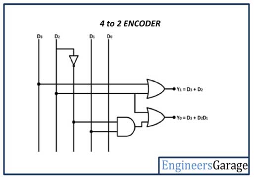 |