The microcontroller only understands digital language. However, the inputs available from the environment to the microcontroller are mostly analog in nature, that is, they vary continuously over time. To understand the inputs of the digital processor, a device called an Analog to Digital Converter (ADC) is used. As the name suggests, this peripheral gathers the analog information provided by the environment and converts it into the controller's understandable digital format, the microcontroller then processes the information and provides the desired result at the output.
((wysiwyg_imageupload:451:))
ATmega16 has an integrated 10-bit, 8-channel ADC system. Some of the basic features of the Armega16 ADC are:
· 8 channels.
· 10-bit resolution.
· Input voltage range from 0 to Vcc.
· 2.56V selectable internal reference voltage source.
· AREF pin for external reference voltage.
· Complete interruption of ADC conversion.
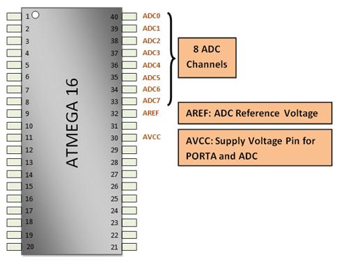
The ADC channels on the Atmega16 are PORTA multiplexed and use the common pins (pin33 to pin40) with PORTA. The Atmega16 microcontroller ADC system consists of the following pins:
I. ADC0-ADC7: 8 channels from pin 40 to pin 33 of the Atmega16 ADC peripheral.
ii. AREF: Pin32 of Atmega16 microcontroller, the voltage at AREF pin acts as reference voltage for ADC conversion, the reference voltage is always less than or equal to the supply voltage i.e. Vcc.
iii. AVCC: Pin30, this pin is the supply voltage pin for using PORTA and ADC; The AVCC pin must be connected to Vcc (microcontroller supply voltage) to use PORTA and ADC.
Note: External reference voltage source can be used on the AREF pin. However, the Atmega16 also has internal reference voltage options of 2.56V and Vref = Vcc.
The figure below shows the pin configuration of the Atmega16 microcontroller ADC system.

Fig. 2: ADC pin numbers on ATmega16 AVR microcontroller
ADC Records
To use the Atmega16 ADC peripheral, certain registers need to be configured.
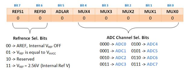
I. ADMUX (ADC Multiplexer and Select Register)

Fig. 3: ADC multiplexer bit values and select register for configuring the ADC peripheral in the AVR
REF(0:1) bits determine the reference voltage source, whether internal or external connected to the AREF pin. The MUX (4:0) bits are used to select between channels that will provide data to the ADC for conversion. The ADLAR bit when set to 1 gives the left-adjusted result in the ADCH and ADCL data registers.
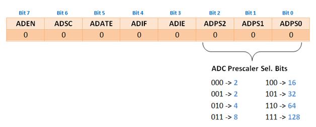
ii. ADCSRA (ADC Control and Status Record)

Fig. 4: ADC control bit configuration and status register in the AVR microcontroller
ÁDEN: ADC enable bit, this bit must be set to 1 to turn on the ADC.
ADSC: ADC Initial Conversion Bit, this bit is set to 1 to start the ADC conversion, once the conversion is complete this bit is set back to 0 by the hardware.
A FIND: ADC Auto Trigger Enable, this bit is set to 1 to enable automatic triggering of the ADC conversion.
ADIF: ADC interrupt flag, this bit is set to 1 when ADC conversion is completed.
ADIE: ADC Interrupt Enable, this bit is set to 1 if we want to enable complete interrupt of ADC conversion.
ADPS(0:2): ADC Prescaler Bits, these bits are used to set the clock frequency of the ADC, the setting of these bits determines the division factor by which the microcontroller clock frequency is divided to get the frequency of the ADC clock. The figure above shows the prescaler bit values for the respective division factor.

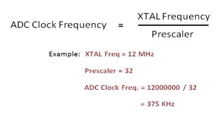
Fig. 5: ADC clock frequency equation
The ADC clock frequency must be between 50 KHz and 200 KHz.
iii. ADCH and ADCL (ADC Data Records)
When the ADC conversion is complete, the data is stored in these two registers. The data configuration depends on the value of the ADLAR bit in the ADMUX register. If ADLAR=0, the data is right-fitted and if ADLAR=1, the data is left-fitted. Always read the ADCL first and then the ADCH. In cases where 8-bit precision is sufficient, set the ADLAR bit to 1 to left-shift the data and read only the ADCH data register.
When ADLAR = 0,

Fig. 6: ADC data register bit setting at ADLAR = 0 on ATmega16 AVR microcontroller
When ADLAR = 1,

Fig. 7: ADC data register bit setting at ADLAR = 1 on ATmega16 AVR microcontroller
Circuit Description
Connect the circuit as shown in the circuit diagram. A ceramic capacitor 104 is connected between AVcc (pin 30) and Aref (pin 32). AVcc (pin 30) is connected to +5V external power.
Code Explanation
To interface the analog device with the AVR microcontroller, follow the steps below to program it.
Step 1: To initialize the ADC
I. Set the value in the ADMUX register according to the ADC channel and reference voltage.
ii. Set the Prescaler bits appropriately in the ADCSRA register.
iii. Set the ADEN bit to enable the ADC.
empty ADC_init(empty) // ADC initialization
Step 2: To read the analog value
I. Enter the channel value in ADMUX
ii. Start the conversion by setting the ADSC bit.
iii. Monitor the ADIF bit for conversion completion.
4. Clear the ADIF conversion bit. When writing 1.
v. The digitally converted result is now available in the ADCH and ADCL registers.
unsigned int ADC_read(unsigned char ch)
{
ch= ch&0b00000111; // the channel must be black and white from 0 to 7
ADMUX = channel; //selecting channel
ADCSRA =(1<Project source code
 ###

 //Program for the ADC to read from channel 0 and show 8-bit o/p in PORTB
###
Project Components
- ATmega16
- LED

