An AC-DC converter is commonly used in many devices. Also called a rectifier, it converts alternating current (AC) into direct current (DC). Most electronic devices, such as computers, smartphones, and electronic circuits, operate on DC power.
However, there are different ways to convert AC power to DC (as discussed in the previous item). AC to CC conversion article).
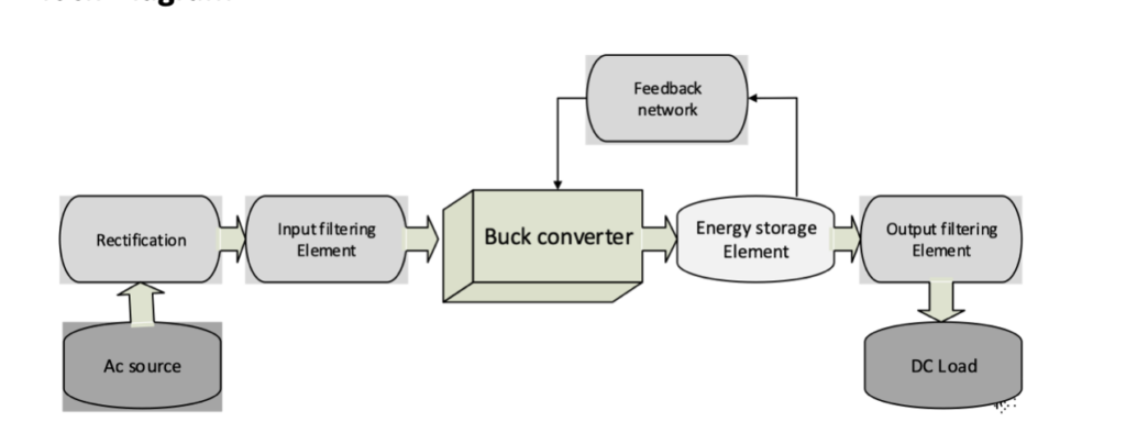
For this project, we will employ a non-isolated topology using a buck converter (see figure 1 ). In a non-isolated power supply, one of the AC power lines is common to the DC ground, so there is no isolation at the input and output.

Figure 1. Block diagram of AC to DC conversion, with non-isolated topology using a Buck converter.
The principle of operation
AC to DC conversion using a buck converter works through switching topology. The internal MOSFET in the converter's integrated circuit (IC) and its oscillator generate the pulse width modulation (PWM) signal, regulating the output voltage through a feedback network.
Conceptually, this is the same principle as a dc-dc buck converter. You can learn more in this switched-mode power supply (SMPS) article, which covers the design of a buck converter.
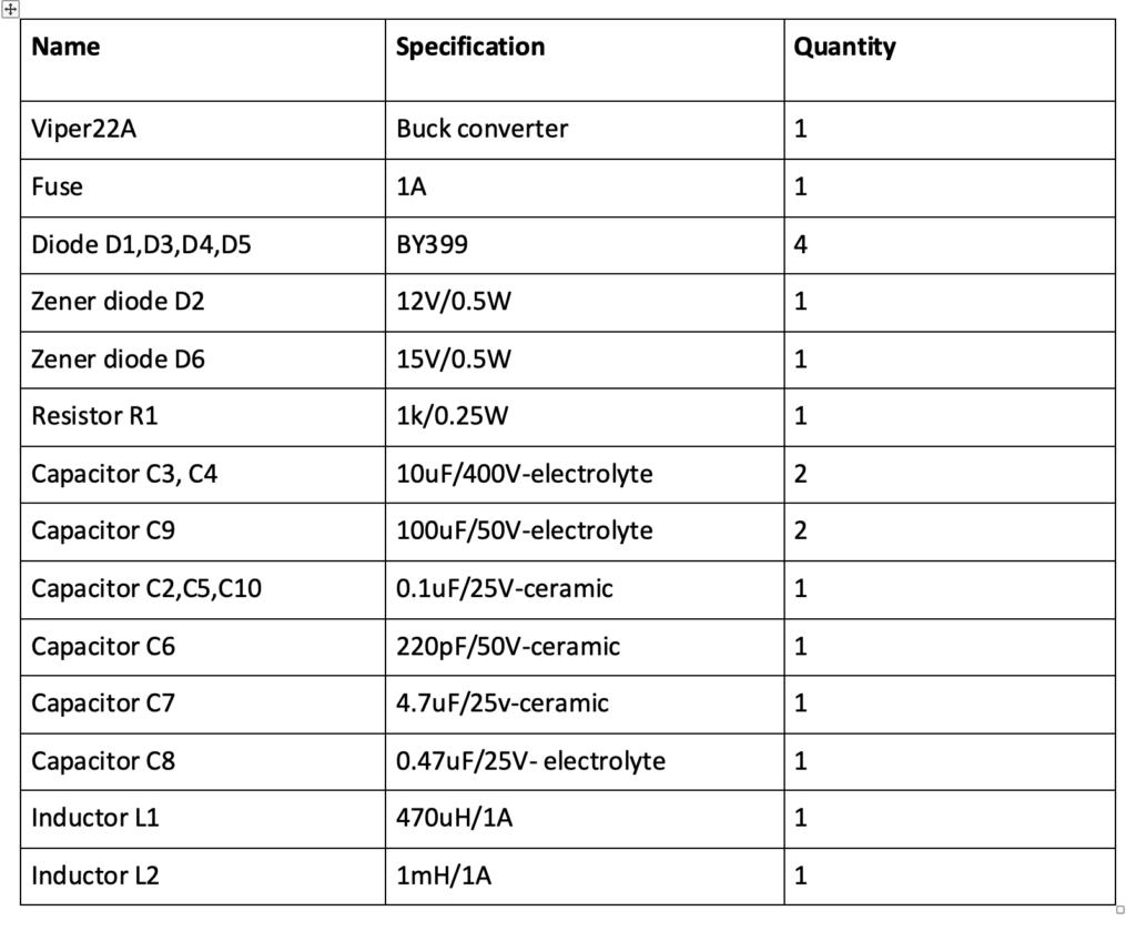
Required components
Circuit Diagram
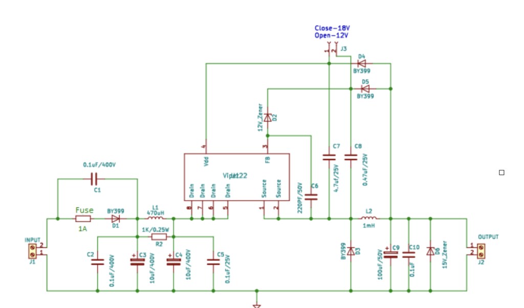
Figure 2. The circuit diagram of an AC to DC conversion using a Buck converter.
Components
 Voltage Regulator – A switching type of regulator should be used for this project because they are more efficient than linear. There are three types of switching regulators: buck, boost and buck boost.
For this application, we will use a Buck IC converter with the following parameters:
- An integrated MOSFET drain voltage
- An operational supply voltage
- Output power
- A non-isolated design
 VIPER22IC – this is a buck converter with a MOSFET and some comparators (see Figure 3 ). Here are its specifications:
- Drain voltage – 730V
- Operating supply voltage – 9 to 38V
- Output power – 12W
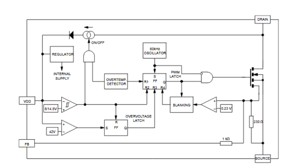
Figure 3. The internal diagram and IC pinout of the Viper22 buck converter.
How it works
- VDD pin – of the IC is used to control the power supply to the internal circuit and provides the charging current in the initial stage. The comparator compares the VDD voltage. For VDD about = 14.5V, the Viper starts to switch. For VDD off = 8V, the Viper stops switching.
- Drain – MOSFET drain and also used by the charging source in the initial stage
- Source – includes the MOSFET source and circuit ground
- Facebook – controls the maximum IC drain current limit
High current protection and rectification
For high starting current and short circuit, a fuse is used on the input side, which burns when the current is greater than 1A.
To convert AC voltage to DC, a half-wave rectifier is used. Diode D1 provided half-wave rectification.
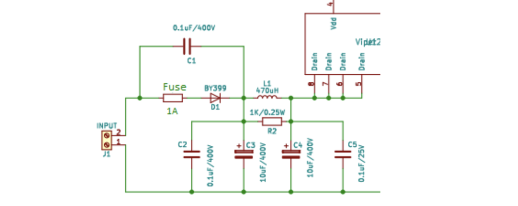
Figure 4. The input filtering circuit diagram.
As per Figure 4 , C1 helps to reduce electromagnetic interference (EMI) noise by balancing the main and neutral lines as it will pass the EN55022 level “B” noise standard (however, if the requirement is lower, this can be ignored) . C2, C3 and L1 form a Pi filter, which also helps reduce EMI noise.
Resistor R2 ensures that the peak current remains low during circuit startup.
Selecting the filtering capacitor
The minimum capacitor voltage must be 1.5 times greater than the AC input voltage. The capacitance is typically two or three times the output power.
So, if the AC input – 220V, then…
The voltage rating of Cin = 2*220 = 440V
If the output power – Vout*Iout = 12*0.1= 1.2 W, then…
Cin = 2*1.2 = 2.4uF
According to availability C3, C4 are 10uF/400V
Selecting the VDD capacitor
Figure 5. The circuit connections for selecting the VDD capacitor.
When the device starts, it will receive some energy from the inductor. Capacitor C7 helps filter and stabilize the VDD voltage. It also sets the IC startup time.
The datasheet recommends a 100nF capacitor. However, considering the output voltage, a 4.7uF/25V capacitor can be used in the circuit. Capacitor C6 also filters the voltage to the FB pin. A small ceramic picofarad works for this project.

Figure 6. The circuit diagram connections for the output diode.
The output diode
The output diode D3 is called a capture or freewheeling diode. In the ON-OFF period of the MOSFET, the inductor passes energy through the diode as output. A fast rectifier diode that is compatible with the frequency of the IC is required. Any drop in the diode causes losses in the circuit, which affects efficiency.
The direct voltage drop:
Rated diode reverse voltage > Vin
Vin (CC) = 220*1.414 = 320V
i.e. V franc > 320V (on the safe side 400V can be used)
We use BY399 diode for this circuit.
Calculation of losses in the BY399 diode:
P d = Forward voltage drop *Iout
Pd = 1*0.1
P d = 0.1 V
Selecting the inductor
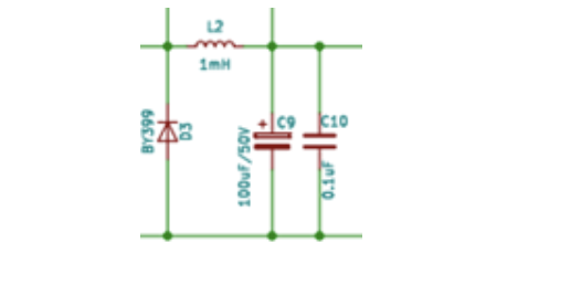
Figure 7. Circuit diagram connects to select inductor.
Inductors L2 and C9 form a filter in the circuit. The inductor output will determine the discontinuous and continuous modes of operation. In continuous mode, losses are greater than in discontinuous mode. To learn more about these two modes, see this article.
The equation below defines the inductor boundary condition for continuous and discontinuous modes. To operate in discontinuous mode, the “L” must be smaller than this:
L = 0.5*R*(1-D)/f
R = output load, 120E
f= IC frequency, 60kHz
D = duty cycle, Vo/Vin= 12/320= 0.0375
L = 1mH(approx.)
We use L2 = 1mH, which suits our design for this project.
Selecting the diodes
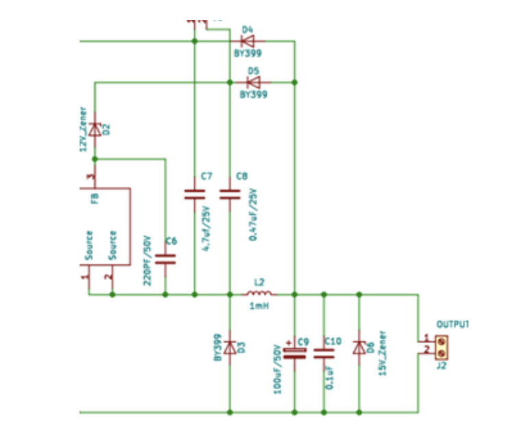
Figure 8. The circuit diagram connections for selecting the Zener diode.
The working circuit
- Drain Voltage – Voltage from capacitor C4 is supplied to the drain of the IC using pins 5 to 8.
- OFF State – When the circuit is initially started, the Viper is not switching. The internal current source in the IC supply is 1mA for the VDD pin. This current charges C7. When the VDD reaches 14.5V, the current sources are turned off and the Viper begins to cycle. During this period, the inductor and output capacitor provide the output power, which is charged to the previous state (ON state).
- On State – In this state, the Viper is switching and the energy stored in C7 is supplied to the output. Therefore, the energy stored in C7 must be greater than that required for the output current. Additionally, there must be power to charge the output capacitor before the VDD drops below 8V. As a result, the charge and discharge time of the C7 is based on the ON and OFF time of the circuit. The inductor also charges through the internal MOSFET and C7 supplies power to the output.
- Freewheeling state – This state occurs with the OFF state. When the VDD voltage drops below 8V (after supplying power to the output), the Viper stops switching (OFF state). Then, the current source will be turned on again and simultaneously the inductor will start discharging through diode D3 (forward biased).
- Output regulation – D2, D5 and C8 regulate the output voltage. During the freewheeling state, D5 carries C8 and D4 carries C7. The source or ground reference is a diode drop, compensating the power at C7 and C8. The output voltage remains the same as the Zener D2 voltage. The D2 is a low current Zener, providing the best accuracy for the output voltage.
Thermal management
For IC heat management, review this article on heatsink selection. It is possible to determine the maximum power dissipation limit of the circuit with or without a heat sink.
Practical observations:
Vin = 220V AC, tested in a closed box, without natural convection
No load, Vout = 14.88V
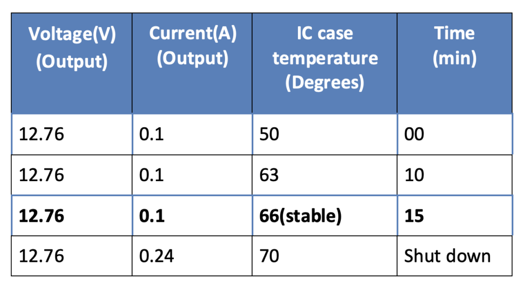
The datasheet states that the IC will shut down if the junction temperature reaches 170 degrees. This circuit will turn off above 100mA of current without natural convection (when closed).
Precautions
- Ceramic capacitors must be used at the input and output for proper filtering as they offer a low ESR.
- A high-power electromagnetic signal may impair the converter's ability to function properly. Inductor operation will stop if a magnetic field interferes.
- Short-circuiting the converter output terminals must be avoided as it may cause permanent damage to the IC.
- The nominal voltage of the capacitor must be 1.5 times greater than the input voltage.
- Fully discharge the capacitor before handling the circuit.
- When handling the circuit, safety gloves are mandatory, especially on the output network line.
- A heat sink can be used for the smooth functioning of the IC.
- Do not use a non-isolated power supply where the load is close to a person.
PCB Design Guidelines
 Keep power strokes thick and short
 Place the input and output capacitor as close as possible to the input and output pins of the IC
 Minimize inductor path length
 Keep voltage and switching nodes away from each other
 Keep all components as close to the IC as possible and try to reduce PCB size
 Note: The higher the IC frequency, the greater the switching losses, which reduces efficiency. However, a higher switching frequency reduces the size of the energy storage element and improves the transient response.
PCB Design
We made the PCB of the circuit using KICAD (see Figure 9 ).
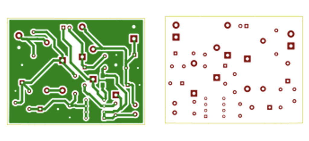
Figure 9. The PCB design of the AC to DC conversion circuit using a buck converter.
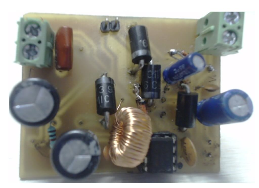
Figure 10. The circuit prototype.


