A DC power supply is used in almost all devices where a regulated voltage is required. A DC converter implements the DC conversion process.
There are two types of DC converters:
- Buck Converter – Reduces input source voltage
- Boost Converter – Increases input source voltage
Conversion topology
- Linear regulator – Can only be used as a Buck converter.
- Switching mode regulator – Can be used as a buck and boost converter.
(Note: For more information on how linear and switching regulators work, see our previous switching power supply and linear regulator power supply series.)
In this experiment, we will design a switch mode buck converter and practically verify the performance curve of the IC.
Specification
- Step down 12V DC to 3.3V DC
- Output current 2A.
Block diagram
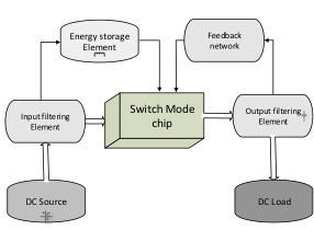
Fig.1 Buck converter block diagram using Switch Mode chip
Required components

Circuit Diagram

Fig. 2 Buck Converter Circuit Diagram
Principle of Operation
AP3512E is a 3.3V Fixed Buck Converter Switching Mode IC. The input voltage range of this IC is 4.5V to 18V. The current continuous output is 2A
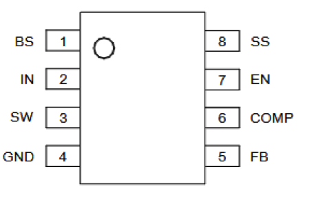
Fig. 3 AP3512E pin diagram
Main Pin Description
EN- It is a digital pin that turns the IC on and off. Drive EN high to ON and low to OFF. For automatic startup I pulled it with a 100k resistor.
SS- Soft start pin is used to control the large inrush current and output overshoots when the circuit is on. SS is usually present in DC to DC converters to make them start up smoothly. Connecting a 0.1uF capacitor to ground sets the SS period to 15ms.
FB– The feedback pin is used to set the output voltage using the resistor divider network. When the FB pin voltage exceeds 1.1V, overvoltage protection is triggered, and when it is below 0.3V, short circuit protection is realized.
The voltage reference of this feedback pin is normally 0.925V, the combination of the reference voltage and resistor divider network will decide the output voltage.
Characteristics
- Overvoltage protection
- Overcurrent protection
- Thermal shutdown
Circuit construction
Setting the output voltage
The output voltage can be calculated by the formula below:
Vout = 0.925(1+R1/R3)
Vout = 3.3V (as it is a fixed 3.3V regulator)
Let's consider R3 = 10k
Now, putting the values in the above equation, we get
R1 = 26.1k approx.
Inductor selection
The wiring diagram consists of an inductor, capacitor and resistor along with the Buck regulator IC. According to the regulator datasheet for a 12V input and a 3.3V output, a 4.7uH inductor is more suitable. The rated current of the inductor must be 1.15-1.25 times greater than the required output current.
The maximum output current that the IC can provide is – 2A
Minimum Inductor Current Rating – 1.15 * 2 = 2.3A
Soft start and filtering
The capacitor at the input and output helps filter the input source, and a 0.1uF capacitor defines the SS period. A feedback capacitor C6 helps stabilize the output voltage at high loads.
(Note: To get a detailed idea about the working of a boost converter, refer to our previous series on SMPS.)
How the circuit works
The regulator in the wiring circuit consists of external components, which are an inductor, a resistor and a capacitor. Internally it consists of a transistor, which acts as a switch.
An inductor is used to store energy in the form of a magnetic field. So, here the inductor acts as an energy storage element. When the circuit is powered with a 12V input source, the regulator starts switching on and off with a frequency of 500 kHz.
During the ON period, the inductor charges and provides a regulated voltage at the output. During the OFF period, the inductor and output capacitor keep the output regulated, releasing the stored energy they store in the ON state. The resistor divider network fixes the output voltage at 3.3V.
Thermal management
The switching regulator is known for its high efficiency and low power dissipation, but as we know this nature is not ideal.
Issuance and rectification
So, we tested a ceramic capacitor in parallel with the feedback pin and output terminal as seen in the schematic (capacitor C6). This works well in our project and the output voltage stabilizes. This capacitor is known as a feedforward capacitor, which adds lead compensation to the feedback circuit and increases the stability of the circuit.
Practical observation
Vin = 12V, Cooling system = Without heatsink and fan
 **We can analyze that at a high current the output voltage starts to increase. This is due to the heating effects of the regulator at high current.
According to your datasheet, the reference voltage increases with increasing temperature. This will further increase your output voltage. To do this, we used the cooling fan to maintain the temperature of the regulator and saw the performance of the regulator at high current. Below are his readings.
Vin = 12V, Cooling system = 12V DC Fan
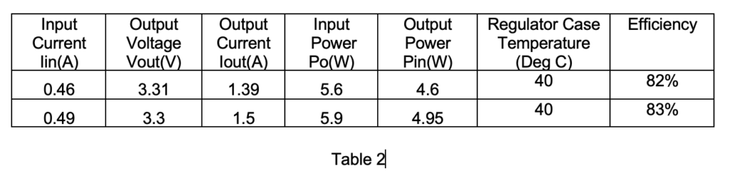

Fig. 4 Load Regulation Curve
Practically observed results vs. datasheet curve

Fig. 5 Image shows practically observed results versus datasheet results
IC performance
- Load regulation – Regulated at 3.3V even with high load.
- Average efficiency of 88% for current > 200mA
Application
1. In digital circuits that require 3.3 V such as microcontrollers.
2. Portable Devices
3. Regulated DC Power
4. Used as an interface between battery and component in CPU or notebooks where voltage demands are lower than battery voltage.
Thermal management
The heating issue is a major problem in a power supply system. To dissipate extra heat from any circuit, various methods can be used such as heat sink, fan or thermoelectric cooler. To find out if our circuit needs any thermal management or not, see our article Power supply thermal management.
Precautions
- A capacitor must be connected between the IN pin and ground to keep the DC input voltage regulated.
- The capacitor used in the circuit must have a higher voltage rating than the input supply voltage. Otherwise, the capacitor will start to leak current due to excess voltage on its plates and will explode.
- For circuit stability, a ceramic capacitor must be connected in parallel with the feedback resistor.
- Make sure all capacitors are discharged before working on a DC power supply.
- The rated current of the inductor must be 1.15 times greater than the output current.
- Do not supply a higher voltage at the IC's input terminal than its operating input voltage range.
- Do not short the output terminals; This will reverse the current flow in the IC and the IC will become faulty.
- Also, do not short the input terminals; This will generate a large current in the circuit and the circuit components will become faulty.
- Frequency effect
High frequency increases switching losses, which decreases the efficiency of SMPS. But the high switching frequency reduces the size of the energy storage element and improves the transient response of the output.
PCB Design Guidelines
- Keep the energy strokes thick and short.
- Place the input and output capacitor as close as the input and output pin of the IC.
- Minimize inductor path length.
- Keep voltage and switching nodes away from each other.
- Keep all components as close as the IC and try to reduce the PCB size
PCB Design Layout

Fig.6 I PCB Design Layout for Buck Converter

Fig. 7 Animated 3D visualization of the PCB
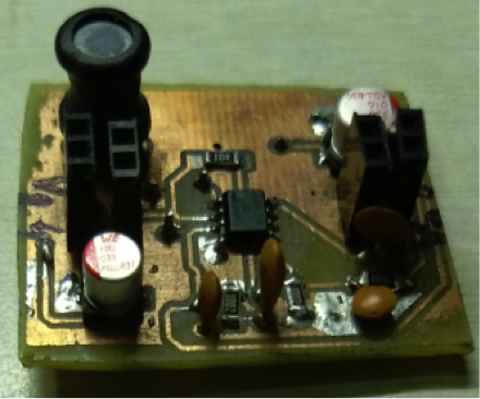
Image. 8 Real view of the PCB
(tagsToTranslate)pic