Many times people face problems while making a circuit on a circuit board. It is a common problem that the circuit works at some time and does not work at another. Most of the time, it is the connections on the breadboard that create this problem. Connections are not suitable or are loose or may be damaged during work or when transporting the circuit on a circuit board. Therefore, it is always recommended to make the circuit on a PCB once tested on a breadboard. But how to make a PCB at home ? This article will explain the process of manufacturing a single layer PCB at home with the use of commonly available tools.
The printed circuit board has pre-engineered copper tracks on a conductive sheet. Predefined tracks reduce wiring, thus reducing faults that arise due to lost connections. Just simply place the components on the PCB and solder them.
Materials Required in PCB Designing :
· Hanging projector sheet (known as OHP sheets) or waxed paper.
· Laser printer.
· Electric iron.
· Steel wool.
· Two plastic trays.
· Copper plate/ PCB (e.g. phenolic paper, epoxy glass, FR4, FR10, etc.)
· Black permanent marker.
· Etching solution (ferric chloride).
· Drill.
Step 1
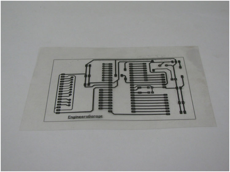
Step 1: Prepare a circuit layout in any commonly used PCB design software. A layout is a project that interconnects components according to the schematic diagram (circuit diagram). Make a mirror print of the layout on the OHP sheet using a laser printer. Make sure the design is correct with proper placement of components.

Fig. 1: Mirror print image of the layout on the OHP sheet
Step 2
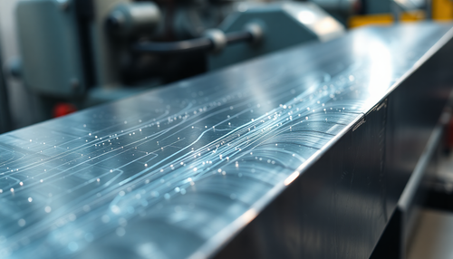
Step 2: Cut the copper plate according to the layout size. A copper plate is the basis of a PCB it can be single layer, double layer or multilayer board.
Single layer copper board has copper on one side of the PCB, it is used to make single layer PCBs, it is widely used by hobbyists or in small circuits. A double layer copper board consists of copper on both sides of the PCB. These boards are generally used by industries. A multilayer board has multiple layers of copper; They are quite expensive and mainly used for complex circuits like PC motherboards.

Fig. 2: Image of a double-layer copper plate
step 3
Step 3: Rub the copper side of the PCB with steel wool. This removes the top copper oxide layer as well as the photoresist layer, if present.

Fig. 3: Image showing copper side of PCB rubbed with steel wool
Step 4
Step 4: Place the OHP sheet (wax paper) that has the layout printed on the PCB sheet. Make sure the printed/mirrored side is placed on the copper side of the PCB.

Fig. 4: Image showing white paper thrown on OHP sheet
Step 5
Step 5: Place a white paper on the OHP sheet and start ironing. The heat applied by the electric iron causes the ink on the OHP sheet traces to stick to the copper plate in exactly the same way as it is printed on the OHP sheet. This means that the copper sheet will now have the PCB layout printed on it. Let the PCB board cool and slowly remove the OHP sheet. As it is a manual process, it may happen that the layout does not appear correctly on the PCB or some of the tracks are broken in the middle. Use the permanent marker and complete the trails correctly.

Figure 5: Image showing ironed OHP sheet covers side of PCB

Figure 6: Image showing pressed OHP iron sheet copper side of PCB

Figure 7: Image showing removal of the OHP sheet from the PCB

Figure 8: Image showing PCB Layout printed on copper PCB side

Figure 9: Image showing PCB Layout printed on copper PCB side

Figure 10: Image showing PCB Layout printed on copper PCB side
Step 6
Step 6: Now the layout is printed on PCB. The area covered by the paint is known as the masked area and the unwanted copper, not covered by the paint, is known as the unmasked area. Now make a ferric chloride solution. Take a plastic box and fill it with some water. Dissolve 2-3 teaspoons of ferric chloride in water. Immerse the PCB in the etching solution (ferric chloride solution, Fecl 3 ) for approximately 30 minutes. Fecl 3 reacts with unmasked copper and removes unwanted copper from the PCB. This process is called Engraving. Use pliers to pull out the PCB and check whether the entire unmasked area has been etched or not. If it is not recorded, leave it in the solution for a while longer.

Fig. 11: Image showing PCB dipped in ferric chloride solution for etching
Step 7
Step 7: Take out the PCB, wash it in cold water and remove the paint by rubbing it with steel wool. The remaining area that has not been engraved is the conductive copper tracks that connect the components as per the circuit diagram.

Fig. 12: Image showing PCB after etching

Figure 13: Image showing PCB cleaned with steel wool

Fig. 14: Image showing copper tracks printed on PCB
Step 8
Step 8: Now carefully drill the PCB using a drill into the pads.

Fig. 15: Image showing holes in the PCB for placing components
Step 9
Step 9: Place the components in the correct holes and solder them.
This completes your PCB Fabrication now place the components on the mounting side and solder them. Be sure to properly dispose of the FeCl3 solution, clean your tools, and wash your hands after this exercise. You can also store the solution in a plastic box for future use, but not for long.