In the previous tutorials, all the circuits designed were combinational circuits . In combinational circuits, the binary output depends only on the current state of the inputs. So actually combinational circuits have static operation. They can have input of a fixed set of values for which the output results in a defined interval at any instant of time.
In practice, most electronic devices have dynamic operation. They process a set of binary information received within a time interval at different instants to effectively produce a relevant, real-time result. To achieve this, electronic devices contain memory elements to store digital information received at a previous instant and have digital circuits that can process information received at the present instant as well as at the previous instant to produce a relevant result. For example, a computer may need to keep the results of a previous calculation aligned for a next calculation.
Thus, the type of digital circuit whose output depends not only on the current state but also on the previous state of the inputs is called a sequential circuit. Sequential circuits are combinational circuits with feedback from memory elements. At any instant, the combinational circuit within a sequential circuit receives the current input and retrieves the previous input states from the memory elements to perform the computation. Once the computation is complete, before the next computation occurs, the combinational part of the sequential circuit stores the currently received input states in memory elements. It can be said that the memory elements in a sequential circuit function as a feedback element. With memory elements at their disposal, sequential circuits are able to store, retain and retrieve the previous state of the inputs or, say, states of the inputs at the previous instant.
There are two types of sequential circuits –
1 ) Synchronous Sequential Circuits
2 ) Asynchronous Sequential Circuits
The two types of sequential circuits differ in the timing scheme of their signals. Synchronous sequential circuits operate on data on periodic clock signals, therefore, they operate on binary data at discrete instants of time. The periodic clock signal is generated by a timing device called a clock generator and the clock signal is generated and received as pulses. The calculation of data by the combinational circuit of the synchronous sequential circuit, as well as the storage and retrieval of data from memory elements, is carried out upon the arrival of clock pulses, i.e. when the clock signal changes from 0 to 1 in such circuits . Meanwhile, the clock signal returns to 0, the combinational circuit of the synchronous circuit prepares for the next computation cycle while the memory elements store the previous state of the inputs and prepare for the same to be recovered upon the arrival of the next pulse. . For synchronous operation of combinational circuits and memory elements according to the periodic clock signal, the propagation delay at the logic gates constructing the respective circuits is controlled accordingly. The rate at which the master clock generates the pulses must be slow enough to allow the slower circuit to respond. This limits the speed of all circuits. It can be said that synchronous circuits are built by integrating combinational circuits, memory elements and a clock generator. A synchronous sequential circuit can be represented by the following block diagram –
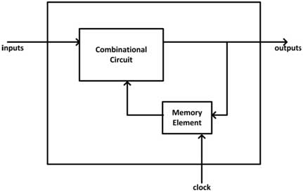
Fig. 1: Block diagram of synchronous sequential circuits
In asynchronous sequential circuits, feedback from previous input states to the combinational circuit can occur at any instant of time, rather than being periodic in nature, and therefore depends on the order of the input signals rather than the occurrence of any pulse. of clock. In these circuits, memory elements are coupled to time delay circuits so that feedback on the previous state of the inputs can be received at the instant the current inputs are received. In most cases, the propagation delay through the gates in the memory elements is sufficient to produce the required time delay. In these circuits, the storage capacity of memory elements also depends on the signal propagation delay. Asynchronous circuits can be unstable or unreliable at times due to unprecedented delays in the circuits or circuit inputs. Therefore, the design of asynchronous sequential circuits always requires caution and extra technical details. Thus, it can be said that asynchronous sequential circuits are built by integrating combinational circuits and memory elements with defined time delays in signal propagation.
Compared to combinational circuits, sequential circuits are slower as they need to synchronize according to clock signal in case of synchronous circuits or must have defined time delays in case of asynchronous circuits. Combinational circuits, since they depend only on the current input states , process the data immediately affected only by the propagation delay of the signals through the gates.
However, sequential circuits incorporate the memory elements that are a vital part of any modern electronics. Most electronic devices need to store or retain data as needed for calculation. Sequential circuits, although speed limited in their own design concept, are the most abundant digital circuits in electronics.
Memory elements –
Memory elements are essential in the construction of any sequential circuit. The simplest memory element can store a single bit at any time. A group of these memory elements forms larger memories. There are two types of single-bit storage memory elements – Latches and Flip-Flops. Both can store a single bit at a time.
Latches are level-sensitive memory elements that respond to the 0 or 1 state of the signal, while flip-flops are transition-sensitive memory elements that respond to the signal's transition from 0 to 1 and vice versa. Responding to signal transitions, flip-flops are called edge-sensitive devices. The flip-flops themselves are constructed from latches. Latches are used as memory elements in asynchronous sequential circuits, but cannot be used in synchronous circuits. In synchronous circuits, flip-flops are used as memory elements.
In a steady state, the output of a flip-flop remains 1 or 0. The output of a flip-flop changes only when a clock pulse is received by it. The output of a flip-flop depends on the current data input or the value currently stored in it or both. The combinational circuit of a synchronous circuit must be synchronized with the clock pulses and reach a stable state before the previous input states are passed to be stored in the flip-flops. The circuit must be able to respond to the change in the states of the flip-flops before the next clock pulse arrives. Therefore, the duration of the clock pulse needs to be predetermined for the proper functioning of a synchronous circuit. It should be noted that these memory elements – latches and flip-flops retain binary information until they receive power. If there is a power cut, the data retained by them at that time is lost.
Locks –
Latches are level-sensitive memory devices. They are used in asynchronous sequential circuits. They are also the building blocks of flip-flops. There are three types of locks –
1 ) SR Lock
2 ) S'R' lock
3 ) D Lock
SR Latch – The SR latch is constructed by two cross-coupled NOR gates. It has two inputs – set (S) and reset (R) while two outputs Q and Q'. OQ and Q' are normally complementary to each other. When the input set is 1 and the input reset is 0, the output Q becomes 1 and Q' becomes 0. When the input set is 0 and the input reset is 1, the output Q becomes 0 and Q' becomes 1. When both set and reset are 0, the SR flip-flop retains the output state, that is, if previously Q became 1 and Q' became 0, the same states will be retained while set and reset are 0. Likewise, if previously Q became 0 and Q' became 1, the same states will be maintained as long as both set and reset are 0. If set and reset are 1, then Q and Q' become 0, the which is prohibited. Therefore, whether set or reset is 1 changes the bit stored by the SR latch, if both become 0, the stored bit is held while both being 1 is a prohibited condition. SR lock can be constructed by NOR gates as follows –
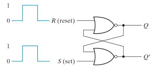
Fig. 2: SR latch logic gate diagram
The operation of an SR lock can be summarized by the following table of functions –
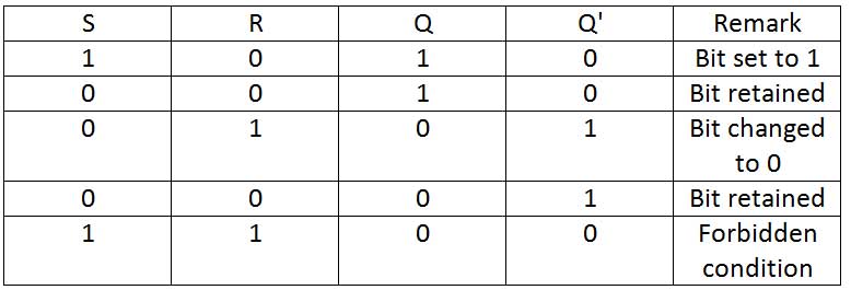
Fig. 3: SR Lock Truth Table
S'R' Latch – The S'R' latch is a type of SR latch constructed from two coupled NAND gates instead of two coupled NOR gates. In S'R' latch, when input set is 1 and input reset is 0, output Q becomes 0 and Q' becomes 1. When input set is 0 and input reset is 1, the output Q becomes 1 and Q' becomes 0. When set and reset are 1, the S'R' flip-flop retains the output state, that is, if previously Q had become 0 and Q' had become 1, the same states will be retained as long as set and reset are 1. Likewise, if previously Q had become 1 and Q' had become 0, the same states will be maintained as long as both set and reset are 1. If set and reset are 0, then both Q and Q' will become 1, which is prohibited. Therefore, if the set or reset value is 0, the bit stored by the S'R' latch will be changed; if both become 1, the stored bit will be retained, while both become 0 is a prohibited condition. It can be seen that the output of the S'R' latch is always a complement to the output of the SR latch, which is why it received its name – S'R' latch. The S'R' latch can be constructed by NAND gates as follows –
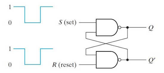
Fig. 4: S'R' lock logic gate diagram
The operation of an S'R' lock can be summarized by the following table of functions –
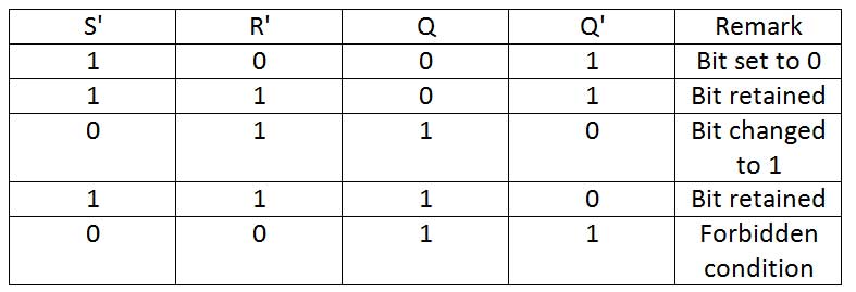
Fig. 5: S'R' Lock Truth Table
The SR or S'R' latch may have additional enable input to control the change in its state. The enable input can be added by connecting two additional NAND gates to the basic SR latch circuit as follows –
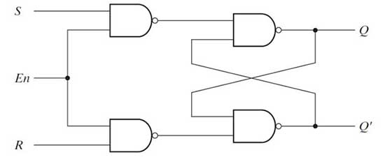
Fig. 6: SR lock logic gate diagram with enable input
The SR lock with enable input has the following function table –
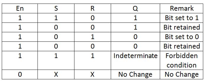
Fig. 7: Truth table of the SR lock with enable input
D Latch – D Latch is a variant of SR latch or S'R' latch to eliminate the prohibited condition from its function table. In a D Latch, there are only two inputs – Data (D) and Enable (En) and there are two outputs Q and Q'. The enable input can be active low or active high. If the enable input is active high, if there is 0 on the enable input, the data will be retained by the latch and will not be transferred to the outputs. When the enable input is set to 1, if the input data is 0, Q becomes 0 and Q' becomes 1, while if the input data is 1, Q becomes 1 and Q' becomes 0. For active high enable input, lock D has the following table of functions –

Fig. 8: Active High D Latch Truth Table
If the enable input is active low, data will be held by the latch when the enable input is set to 1 and transferred to the output when the enable input is set to 0. The enable input can be made active at low level by connecting an inverter port to it. With low enable input active, the D Latch has the following function table –

Fig. 9: Low D Active Latch Truth Table
AD The latch is constructed by coupling the input to the NAND gates in an SR latch with Enable input. By coupling the NAND gates at the first logic gate implementation level of the D latch, the data input is directly connected to the Set (S) input of the SR latch while it is connected through an inverter to the Reset (R) input of the SR latch . This way, when Data (D) is 0, Set is 0 and Reset is 1, whereas when D is 1, Set is 1 and Reset is 0. AD latch has the following logic gate diagram –
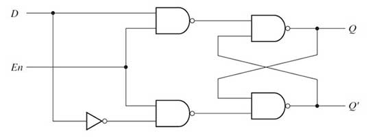
Fig. 10: D lock circuit diagram
As in a D latch, data is transferred to the Q output when Enable (En) is set to 1 in case of active high or is set to 0 in case of active low setting while being held in the reverse state of the enable input, the D lock is also called transparent lock.
Latches are used as memory elements in asynchronous sequential circuits. In the next tutorial, Flip-flops and their different types will be discussed. Flip-flops are the memory elements used in synchronous sequential circuits.

