ADC with NRF24LE1
We studied the first NRF module program which was very simple and we were successful in blinking the LED .
Now if we want to do anything with NRF, we must know how to receive analog inputs as most of the sensor is analog. In this article, we will see how to use NRF's built-in ADC and how we can use any analog sensor and convert its value to digital

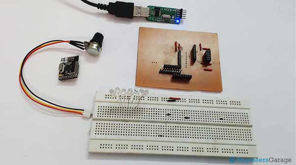
Fig. 1: NRF24LE1 interface prototype with ADC
Some important specifications about the NRF24LE1's built-in ADC are:
• 6, 8, 10 or 12 bit resolution – Means we have the option to choose 6, 8, 10 or 12 bit ADC.
• 14 input channels – 14 input pins for analog input signal
• Single-ended or differential input – Single-line input or two-line input
• Full scale range defined by internal reference, external reference or VDD – To define the maximum analog voltage to be detected.
• Single step mode – Convert the signal and then stop
• Continuous mode with sampling rate of 2, 4, 8 or 16 kbps – Continuously converts the signal unless interrupted.
• Low current consumption; just 0.1 mA at 2 kbps

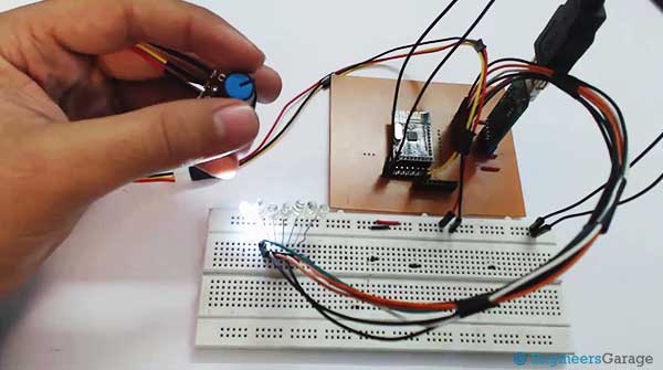
Fig. 2: Image showing the interface of NRF24LE1 with ADC
These are the specifications we extracted from the datasheet. Now, to understand the code, we take a snippet from the example codes provided by Nordic. Let's understand the main part of the code line by line.
Functions provided by the Nordic library
| FUNCTION NAME | INPUT PARAMETER | EXIT | DESCRIPTION |
|---|---|---|---|
| hal_adc_set_input_channel | AIN0 – AIN13 | – | Set the input channel |
| hal_adc_set_reference | INT/VDD/AIN3/AIN9 | – |
Set the reference voltage INT – Internal reference of 1.22V VDD – 3.3V reference AIN3/AIN9 – external reference |
| hal_adc_set_input_mode |
UNIQUE/DIFF_AIN2/ DIFF_AIN6 |
– |
Set the input type SINGLE – Single-ended input DIFF_AIN2 – Differential input with AIN2 as inverting input DIFF_AIN6 – Differential input with AIN6 as inverting input |
| hal_adc_set_conversion_mode | SINGLE_STEP/CONTINUOUS | – |
Set the conversion mode SINGLE_STEP – single step CONTINUOUS – Continuous |
| hal_adc_set_resolution |
RES_6BIT/ RES_8BIT/ RES_10BIT/RES_12BIT |
– |
Set ADC resolution RES_6BIT – 6-bit resolution RES_8BIT – 8-bit resolution RES_10BIT – 10-bit resolution RES_12BIT – 12-bit resolution |
| hal_adc_set_data_just | ONLY_LEFT/ONLY_RIGHT | – |
Justify the position of the output data JUST_LEFT – Left position JUST_Right – correct position |
| hal_adc_start | – | – | Start ADC conversion |
| hal_adc_busy | – | 0/1 |
Check conversion status 0 – Not busy 1 – Busy |
| hal_adc_read_LSB | – | Byte | Read the LSB of the converted data |
| hal_adc_read_MSB | – | Byte | Read the MSB of the converted data |
//Configure the ADC
hal_adc_set_input_channel (HAL_ADC_INP_AIN0);
Here we need to assign which input pin we are configuring for the analog input. Since we are using P0.0, we define this by HAL_ADC_INP_AIN0
hal_adc_set_reference (HAL_ADC_REF_VDD);
The ADC reference voltage is kept equal to VDD (supply voltage), which is 3.3V
hal_adc_set_input_mode (HAL_ADC_SINGLE);
Since we are using a single entry, it is set to HAL_ADC_SINGLE.
hal_adc_set_conversion_mode (HAL_ADC_SINGLE_STEP);
During ADC conversion, we can set the conversion mode. Here we define as single step
hal_adc_set_resolution (HAL_ADC_RES_8BIT);
We can also set the resolution before the controller starts ADC operations. We are setting it to 8 bits
hal_adc_set_data_just (HAL_ADC_JUST_RIGHT);
We can adjust the data to the right or left in the ADC operation. We're adjusting to the right
Find below the main loop where the ADC operation is taking place
Project source code
###
//Program to/* Copyright (c) 2009 Nordic Semiconductor. All rights reserved.
*
###
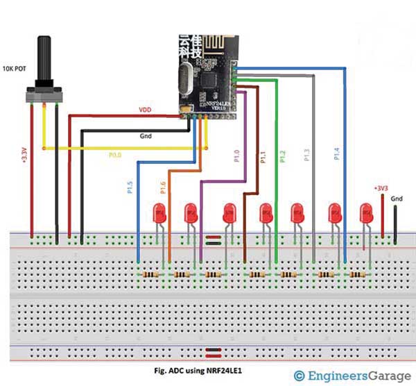
Circuit diagrams
| Circuit Diagram-NRF24LE1-Interface-ADC |  |
Project video

